- Home
- About Journals
-
Information for Authors/ReviewersEditorial Policies
Publication Fee
Publication Cycle - Process Flowchart
Online Manuscript Submission and Tracking System
Publishing Ethics and Rectitude
Authorship
Author Benefits
Reviewer Guidelines
Guest Editor Guidelines
Peer Review Workflow
Quick Track Option
Copyediting Services
Bentham Open Membership
Bentham Open Advisory Board
Archiving Policies
Fabricating and Stating False Information
Post Publication Discussions and Corrections
Editorial Management
Advertise With Us
Funding Agencies
Rate List
Kudos
General FAQs
Special Fee Waivers and Discounts
- Contact
- Help
- About Us
- Search


The Open Cybernetics & Systemics Journal
(Discontinued)
ISSN: 1874-110X ― Volume 12, 2018
Fast Radix-2 Sequential Multiplier Using Kintex-7 FPGA Chip Family
Qasem Abu Al-Haija1, *, Sharifah M. S. Ahmad2
Abstract
Subheading:
Benchmarking of Radix-2 Sequential Multiplication using five Xilinx FPGA families.
Background:
This paper presents description on the implementation of fast radix-2 sequential multiplier using repeated carry save addition (CSA) method with variable data path sizes ranging from 8 bits to 1024 bit.
Objective:
The main objective of this paper is to achieve the best achievable time delay reduction with better performance (i.e. frequency) running on FPGA platforms and prove their applicability in high performance reconfigurable computing.
Methods:
The design was implemented using VHDL description language and synthesized using five different Xilinx FPGA chip families, namely: vertix7, kintex7, artix7, zynq7 and spartan6. Rigorous tests were conducted and analyzed in terms of maximum frequency and total delay time of the FPGA design as well as the hardware utilization.
Results:
The results on the code synthesizing demonstrated that the proposed 1024-bit sequential multiplier with kintex7 chip family outperforms others with a maximum frequency of 296 MHz, while Spartan 6 recorded the lowest frequency with 140 MHz.
Conclusion:
The performance of the proposed multiplier-based CSA was benchmarked against other state-of-the-art designs which results reflected its superiority in terms of throughput of two or more multiple times as compared to others.
Article Information

Identifiers and Pagination:
Year: 2018Volume: 12
First Page: 30
Last Page: 41
Publisher Id: TOCSJ-12-30
DOI: 10.2174/1874110X01812010030
Article History:
Received Date: 12/09/2017Revision Received Date: 12/02/2018
Acceptance Date: 13/02/2018
Electronic publication date: 09/03/2018
Collection year: 2018
open-access license: This is an open access article distributed under the terms of the Creative Commons Attribution 4.0 International Public License (CC-BY 4.0), a copy of which is available at: (https://creativecommons.org/licenses/by/4.0/legalcode). This license permits unrestricted use, distribution, and reproduction in any medium, provided the original author and source are credited.
* Address correspondence to this author at the Department Electrical Engineering, King Faisal University, Ahsa, 31982, P. O. 380, Saudi Arabia; Tel; +966135895400; E-mails: Qalhaija@kfu.edu.sa, Eng_Qasem1982@Yahoo.com
| Open Peer Review Details | |||
|---|---|---|---|
| Manuscript submitted on 12-09-2017 |
Original Manuscript | Fast Radix-2 Sequential Multiplier Using Kintex-7 FPGA Chip Family | |
1. INTRODUCTION
The remarkable progress in electronic technology has led to an enormous impact on digital integrated circuits industries. Digital Integrated circuits are usually designed by engineers using Electronic Design Automation (EDA) [1E.D. Automation, "About the EDA Industry", Electronic Design Automation Consortium, 2015 http://www.edac.org] software. EDA develop the hardware environment using the HDL (Hardware Description Language) as designing language along with the FPGA (Field Programmable Gate Arrays) chip as the target device, to realize the automation of electronic products design. FPGAs are integrated circuits that enable designers to program customized digital logic with its own microprocessors, memory blocks, and interfaces. It permits more flexibility in the hardware design due to the ease of building any digital system using the three basic blocks (i.e. wire, a logic gate, and a register) and the ability to change the system functionalities without introducing a large amount of cost and risk of delays into the design schedule [2C. Maxfield, “The Design Warrior’s Guide to FPGAs: devices, tools and flows”, Mentor Graphics Corporation and Xilinx., Elsevier, 2004]. FPGA chips contain a matrix of Configurable Logic Blocks (CLBs) connected via programmable interconnects that can be configured in the field (i.e. as name implied) using HDLs such as VHDL [3D.L. Perry, "VHDL: Programming by Example", 4th ed., the McGraw-Hill Companies, 2002] which stands for VHSIC (Very High Speed Integrated Circuit) Hardware Description Language along with EDA simulation and synthesizing tools.
Nowadays, FPGAs are efficiently used to develop applications specific co-processors such as the design of high performance multiplier with large data path size such as 512 or 1024 bits. Indeed, a multiplier is an essential unit in many digital signal and embedded processing applications such as image processing, Fast Fourier Transform (FFT), in microprocessors design (i.e. in ALU design), crypto-processors design etc. As multiplication operation consumes most of the execution time of many DSP algorithms, therefore, a fast multiplier design and implementation is highly on demand. Implementing an efficient multiplication algorithm aims to enhance different design factors such as decreasing the total execution time (thus increasing the multiplier speed), improving the design area (i.e. decrease the number of gates and registers) and minimizing the power consumption (especially for energy aware applications).
The fast multiplication unit is required by several DSP and Embedded system design. Many investors are targeting the design of fast multiplications. All the techniques that are reviewed in the survey are recently published or patent-applied innovative techniques for improving the performance/cost complexity of multiplication operation. For instance, inventors of US patent no. 8099655 b1 presented a sequential Galois field (GF) multiplication multiplier system and method [4K.H. Tan, and A. Wassal, "Galois field multiplier system and method", US Patent 8099655 B1, Jan 17, 2012] which can enhance the computation of elliptic curve cryptography over GF (p) [5Q. Abu Al-Haija, and A. Al Badawi, "Cost-effective design for binary Edwards elliptic curves crypto-processor over GF (2N) using parallel multipliers and architectures", International Journal of Information and Computer Security, Inderscience, vol. 5, no. 3, pp. 236-250.
[http://dx.doi.org/10.1504/IJICS.2013.055840] ] while general purpose large multipliers and another binary multiplier circuit for programmable logic devices have been invented recently to be implemented in programmable logic devices in the us patents [6R. Goyal, A.K. Dey, and N. Gupta, "Binary adder and multiplier circuit", US Patent 8933731 B2, Jan 13, 2015, 7M. Langhammer, and K. Tharmalingam, "Large multiplier for programmable logic device", US Patent 8788562 B2, Jul 22, 2014] respectively. Many other works have been listed in the literature for multiplier design-based FPGA targeting these factors [8M.M. Kamble, and S.P. Ugale, "Analysis of different multiplication algorithm and FPGA implementation of recursive barrel shifter method for multiplication", International Research Journal of Engineering and Technology, vol. 3, no. 1, pp. 1141-1142.-31A. Kareem, M. Vardhana, and P. Kumar, "VLSI Implementation of High Speed-Low Power-Area Efficient Multiplier Using Modified Vedic Mathematical Techniques", Recent Patents on Computer Science, vol. 9, no. 3, pp. 216-221.
[http://dx.doi.org/10.2174/2213275908666150220203501] ]. Xilinx corporation for FPGA design industry provides different programmable FPGA chipsets to address the requirements across a wide set of applications with system integration while optimizing for performance/watt [32 Available from https://www.xilinx.com/products/silicon-devices/fpga.html] such as Kintex, Virtex, Spartan and other FPGA chip families. Such applications may range from high-performance networking applications that require the highest capacity, bandwidth, and performance to small-low-cost, footprint FPGA applications. The complete details about the internal architecture and specifications for each FPGA family can be found from [32 Available from https://www.xilinx.com/products/silicon-devices/fpga.html].
In this work, we propose an efficient FPGA implementation for the radix-2 sequential multiplication of variable precision data-path sizes. In this work, we have used the iterative shift-and-add algorithm that has less number of hardware units based on Carry Save Adder (CSA) as an internal adder which provides the multiplication results in redundant form. Then, we retrieved the conventional results using two methods: using two times CSA or using one time Carry Lookahead Adder (CLA). Another non-conventional number representation system can be used instead of CSA to design similar sequential multiplier is the use of Sign-Digit form such as the Canonical Signed Digit (CSD) multiplier invented in [33A. Saado, "Canonical signed digit (CSD) coefficient multiplier with optimization",US Patent 7680872 B2, Mar 16, 2010]. The main objective of this paper is to achieve the best achievable time delay reduction with better performance (i.e. frequency) running on FPGA platforms and prove their applicability in high performance reconfigurable computing. We have compared our results with many optimized implementations [22A. Sharma, "FPGA Implementation of a High-Speed Multiplier Employing Carry Lookahead Adders in Reduction Phase", International Journal of Computer Applications, vol. 116, no. 17, .-30V. Škobic’, B. Dokic’, and E. Ivanovic’, "FPGA Implementation of Montgomery Modular Multiplier", 5th Small Systems Simulation Symposium, Serbia, .]. We have used Xilinx ISE synthesis tool, Modalism SE simulation tool, and Xilinx Kintex-7 (the major platform of this implementation), Virtex-7, Artix-7, Zynq-7, and Spartan-6 FPGA platforms for implementation and benchmarking purposes. We provided extensive comparisons between our proposed designs and other state-of-the-art implementations [22A. Sharma, "FPGA Implementation of a High-Speed Multiplier Employing Carry Lookahead Adders in Reduction Phase", International Journal of Computer Applications, vol. 116, no. 17, .-30V. Škobic’, B. Dokic’, and E. Ivanovic’, "FPGA Implementation of Montgomery Modular Multiplier", 5th Small Systems Simulation Symposium, Serbia, .] in terms of performance efficiency and area.
The remaining of this paper is organized as follows: Section 2 discusses the related works for multiplication design. Section 3 provides a brief background about sequential multiplication, carry save addition, carry lookahead addition and overview of Xilinx FPGA families' comparison. Section 4 discusses the complete hardware implementation and specifications with further processing of multiplication. Section 5 contains experimental results together with the discussions which include performance measures and hardware utilization of the proposed designs in addition to the comparisons with previously reported implementations. Finally, Section 6 concludes the paper.
2. RELATED WORK
In the recent years, several hardware and software solutions try to address the efficient design of digital arithmetic algorithms such as digital multipliers. The most commonly used solutions were based on the FPGA design and synthesize with its various chip families, which was the dominator method of implementing high-speed arithmetic processor. Here, we present a thorough and critical review of work conducted in [8M.M. Kamble, and S.P. Ugale, "Analysis of different multiplication algorithm and FPGA implementation of recursive barrel shifter method for multiplication", International Research Journal of Engineering and Technology, vol. 3, no. 1, pp. 1141-1142.-21P. Agrawal, and R. Sinha, "Comparative Analysis and FPGA Implementation of Vedic Multiplier for various Bit Lengths using Different Adders", International Journal of Innovative Research in Computer and Communication Engineering, vol. 3, no. 10, p. 29., 31A. Kareem, M. Vardhana, and P. Kumar, "VLSI Implementation of High Speed-Low Power-Area Efficient Multiplier Using Modified Vedic Mathematical Techniques", Recent Patents on Computer Science, vol. 9, no. 3, pp. 216-221.
[http://dx.doi.org/10.2174/2213275908666150220203501] ]. Also, many other related researches were not discussed in this section, instead they are mentioned in the results and comparisons section for benchmarking and comparison purposes [18D.J. Udhani, and R.C. Patel, "Implementation of high speed multiplier on FPGA", International Journal of Science, Engineering and Technology Research, vol. 3, no. 2, .-26K. Babulu, and G. Parasuram, "FPGA Realization of Radix-4 Booth Multiplication Algorithm for High Speed Arithmetic Logics", International Journal of Computer Science and Information Technologies, vol. 2, no. 5, pp. 2102-2107.].
Vedic multiplication techniques have been widely used, implemented and discussed in the last five years [4K.H. Tan, and A. Wassal, "Galois field multiplier system and method", US Patent 8099655 B1, Jan 17, 2012-7M. Langhammer, and K. Tharmalingam, "Large multiplier for programmable logic device", US Patent 8788562 B2, Jul 22, 2014, 11S. Tamilselvan, "Design, Analysis and FPGA Implementation of N Bit Vedic Multiplier Based on Different Adder Architectures", International Journal of Advanced Research in Computer and Communication Engineering, vol. 4, no. 8, pp. 72-76.-14R. Pradhisha, "FPGA Implementation of Self-Testing Logic gates, Adders and Multipliers", Indian Journal of Science and Technology, vol. 8, no. 22, pp. 23263-23271.
[http://dx.doi.org/10.17485/ijst/2015/v8i22/79331] , 17S. Khatri, and G. Jangid, "FPGA Implementation of 64-bit fast multiplier using barrel shifter", International Journal for Research in Applied Science and Engineering Technology, vol. 2, no. 7, pp. 86-95.]. For instance, Abdulkareem, M. Vardhana, and P. Kumar [30V. Škobic’, B. Dokic’, and E. Ivanovic’, "FPGA Implementation of Montgomery Modular Multiplier", 5th Small Systems Simulation Symposium, Serbia, .] proposed FPGA implementation efficient multiplier using modified Vedic mathematical techniques. They implemented and tested their designed using Cadence Encounter Xilinx tool which proved the efficient use of Vedic Sutra as they comparison reports revealed that their multiplier consumes less time and is faster than the existing multipliers as well as consumes less power than the existing multipliers. Also, M. M. Kemble and S. P. Ugale [4K.H. Tan, and A. Wassal, "Galois field multiplier system and method", US Patent 8099655 B1, Jan 17, 2012] implemented the digital multiplier using barrel shifter. They described their hardware using VHDL and targeted Xilinx xc3s400 FPGA as a hardware platform as well as simulated the implementation using Xilinx ISE-simulation tool. Finally, they compared their work with different multipliers in terms of cost, power consumption, area and speed and concluded that the use of barrel shifter enhances the design for all these measurements. On the other hand, Rakesh and Shilpa [5Q. Abu Al-Haija, and A. Al Badawi, "Cost-effective design for binary Edwards elliptic curves crypto-processor over GF (2N) using parallel multipliers and architectures", International Journal of Information and Computer Security, Inderscience, vol. 5, no. 3, pp. 236-250.
[http://dx.doi.org/10.1504/IJICS.2013.055840] ] proposed 64-bit multiplier-based VEDIC multiplication method and carry save addition technique with less number of gates and high-speed specification. They synthesized their implementation using Xilinx XST. They concluded that their proposed architecture was highly fast and accurate.
Also, S. Thawait and J. Verma [6R. Goyal, A.K. Dey, and N. Gupta, "Binary adder and multiplier circuit", US Patent 8933731 B2, Jan 13, 2015] presented a simplified and efficient method of multiplication using Vedic mathematics based on Urdhva Triyakbhyam’s Sutra. They synthesized their VHDL implementation using Xilinx ISE 9.2i simulator and found that Urdhva Triyakbhyam sutra of Vedic multiplication is to be the most efficient sutra amongst its all 16 sutras. On the other hand, S. Tamilselvan, et al. [7M. Langhammer, and K. Tharmalingam, "Large multiplier for programmable logic device", US Patent 8788562 B2, Jul 22, 2014] implemented an Urdhva Tiryakbhyam’s sutra method of Vedic multiplication based on Carry select addition. They reported the performance of their multiplier produced less time delay than carry look ahead adder, ripple carry adder, carry skip adder and carry select adder. They described their design using Verilog HDL and simulated using Xilinx ISE 14.3 software targeting Spartan 6 FPGA devices. They recorded a delay time of their 16-bit design 23.47 ns which is considered faster than the conventional multiplier which produce a delay 41.055 ns as they used in Fast Fourier Transform algorithm.
In addition, Kishore et al. [15V. Satya Kishore, J.E. Abhilash, and G.N. Ratnakishor, "FPGA Implementation & Performance Comparison of Various High Speed Unsigned Binary Multipliers using VHDL", International Journal on Recent and Innovation Trends in Computing and Communication, vol. 2, no. 12, .] studied different types of multipliers by comparing their speeds and areas. They developed the VHDL coding to implement multipliers like WTM, Dadda Multiplier, Vedic Multiplier, Computation Sharing Multiplier (CSHM), Serial Multiplier and Multipliers using different compressors in Wallace tree architecture. They tested their 8-bit design using XILINX ISE Simulator targeting the FPGA device xc3s500e-5pq208 and found that the maximum power consumption has been recorded for CSHM multiplier. On the contrary, Vedic multiplier outperformed with the least power consumption. While the fastest multiplier was found to be Wallace tree multiplier with 13.4 ns time delay. The case was different in [16V. Kunchigi, L. Kulkarni, and S. Kulkarni, "High Speed and Area Efficient Vedic Multiplier", International Conference on Devices, Circuits and Systems (ICDCS), pp. 360-364.
[http://dx.doi.org/10.1109/ICDCSyst.2012.6188747] ] where the authors proposed high speed pipelined multiplier that consists of 3 stages. The first, second and third stages consist of a 4 - bit Vedic multiplication unit, a parallel generation of partial products to eliminate unwanted multiplication steps and carry, and adders that built up a multiplication process respectively. They modeled their proposed algorithm using Verilog hardware description language. Their simulation results were carried on Xilinx FPGA device, Spartan-3E and showed that 11 logic cells were required to build nibble multiplier whereby the propagation time of the proposed architecture was found to be 4.585ns. They also concluded that the multiplier implemented using Vedic multiplication was efficient in terms of area and speed as compared to its implementation using Array and Booth multiplier architectures.
Alternatively, in [17S. Khatri, and G. Jangid, "FPGA Implementation of 64-bit fast multiplier using barrel shifter", International Journal for Research in Applied Science and Engineering Technology, vol. 2, no. 7, pp. 86-95.], S. Khatri and G. Jangid described the hardware implementation of a 64-bit Urdhva-triyagbhyam’s sutra of Vedic multiplier based on Barrel shifter using VHDL and targeting the FPGA device SPARTAN 3E 3S 250E. Their results on synthesizing has reported a total path delay of 315.725 ns for the proposed Vedic multiplier. Similarly, D. J. Udhani and R. C. Patel in [18D.J. Udhani, and R.C. Patel, "Implementation of high speed multiplier on FPGA", International Journal of Science, Engineering and Technology Research, vol. 3, no. 2, .] proposed a high-speed multiplier design for convolution, discrete Fourier transform, digital filters, and other digital signal processing operations. Accordingly, they used a 4x4 bit and 8x8 Urdhva Tiryagbhyam Sutra version of Vedic multiplication with different schemes. Among the several schemes of 4x4 multipliers, their new 4bit adder recorded the best delay time with 17.7 ns while for the 8x8 multiplier the best delay time was listed as 30.4 ns.
P. Agrawal and R. Sinha in [21P. Agrawal, and R. Sinha, "Comparative Analysis and FPGA Implementation of Vedic Multiplier for various Bit Lengths using Different Adders", International Journal of Innovative Research in Computer and Communication Engineering, vol. 3, no. 10, p. 29.] described the design of Vedic multiplier based on Urdhva Trigbhyam technique of multiplication. They compared the design of Vedicmultiplier for different bit lengths based on Ripple Carry Adder and Kogge Stone Adder and found that Kogge Stone Adder performed fastest with Parallel Prefix Adder. Hence the delay in Vedic Multiplier based on Kogge Stone Adder is less as compared to that based on Ripple Carry Adder. Also, they tested their implementation using Spartan6, device as xc6slx45, package csg324 with speed grade of -3 and found that the delay for 16-bit Vedic Multiplier using Ripple Carry Adder has been found to be 29.051 ns whereas using Kogge Stone Adder has been found to be at 27.499ns.
On the other hand, M. H. Al Mijalli [12H. Mohammed, and Al Mijalli, "Spartan-3A FPGA Implementation", World Applied Sciences Journal, vol. 18, no. 9, pp. 1291-1295.] presented VHDL implementation for Braun’s multipliers with four-bit lengths; 4×4, 6×6, 8×8 and 12×12 respectively. They target four Spartan-3A FPGA devices; namely: XC5S50A (package: tq144, speed grade: -5), XC3S200A (package: ft256, speed grade: -5), XC3S400A (package: Fg400, speed grade: -5), and XC3S700A (package: fg484, speed grade: -5). The compared their results with the synthesizing report for all devices and found that all the targeted devices have the same number of 4-LUTs, occupied slices, bonded IOBs, total equivalent gate count but their average connection and maximum pin delays were different. The comparison for 12x12 multiplier reported that using Spartan-3A XC3S400A (Package: fg400, speed grade: -5) has the best results in terms of maximum pin delay with 3.2 ns.
Also, V.R. Raut and P. R. Loya in [13V.R. Raut, and P.R. Loya, "FPGA Implementation of Low Power Booth Multiplier Using Radix-4 Algorithm", International Journal of Advanced Research in Electrical, Electronics and Instrumentation Engineering, vol. 3, no. 8, .
[http://dx.doi.org/10.15662/ijareeie.2014.0308081] ] proposed a VHDL design and implementation of radix 2 and modified radix 4 Booth multipliers to enhance the power consumption and delay time. Because of their comparison, they found that the modified radix 4 Booth multipliers have reduced power consumption than the conventional radix 2 Booth Multiplier. However, researchers of [14R. Pradhisha, "FPGA Implementation of Self-Testing Logic gates, Adders and Multipliers", Indian Journal of Science and Technology, vol. 8, no. 22, pp. 23263-23271.
[http://dx.doi.org/10.17485/ijst/2015/v8i22/79331] ] presented self-checking FPGA designs using VHDL for arithmetic and logic circuits, such as single-bit full adder, 4-bit adder and 2-bit multiplier circuits with target chip EP2C20F484C7 Altera Cyclone-II. They applied different test data input samples through input switches, while the error status results were obtained on the 7-segment display device. Thus, they found that the probability of error occurrence increases for complex designs, but this error occurrence can be avoided by using self-checking circuits at different build stages in the complex circuit model. Furthermore, S. Kaur and P. S. Jassal [19S. Kaur, and P.S. Jassal, "FPGA Implementation of Double Precision Floating Point Multiplier using Xilinx Coregen Tool", International Journal of Electronics and Computer Science Engineering, vol. 2, no. 3, .] proposed three different FPGA implementations based DSP48s (No DSP48s, 16 DSP48s, and 17 DSP48s) of 64-bits double precision floating-point multiplier using Xilinx Coregen tool. From all the three implementations, they concluded that as the use of DSP48s was increased, the usage of LUTs and FFs decreased whilst the speed and latency increased. Therefore, the use DSP48s was found to reduce the design cycle by a large factor. Other state of the art work [22A. Sharma, "FPGA Implementation of a High-Speed Multiplier Employing Carry Lookahead Adders in Reduction Phase", International Journal of Computer Applications, vol. 116, no. 17, .-30V. Škobic’, B. Dokic’, and E. Ivanovic’, "FPGA Implementation of Montgomery Modular Multiplier", 5th Small Systems Simulation Symposium, Serbia, .] was mentioned in section 5 of Results and Discussions.
Unlike the aforementioned works, the main objective of our work focuses on efficient FPGA implementation and synthesize of sequential multiplier using different data-path sizes and FPGA device technologies in terms of timing issues such as the total delay period and maximum frequency as well as the hardware utilization percentage of the digital processor. In this paper, we present description on the proposed sequential multiplier-based CSA adder using kintex7 FPGA kit family via VHDL as main target device. In addition, a comparative synthesizing study was carried out on several design options using different FPGA devices in terms of delay and maximum frequency. The comparison with other existed designs showed that the proposed coprocessor design has a throughput efficiency of two or more multiple times faster than other designs.
3. BRIEF BACKGROUND
Typical sequential multiplier algorithm can be designed using two major techniques: right-shift algorithm and left-shift algorithm. For instance, we'll review the right shift algorithm. Let’s assume that:
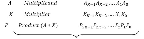 |
The basic multiplication equations can be derived as: P = A.X, where:
 |
Using right shift-and- add algorithms, we get:
 |
The mathematical model of sequential shift-and-add multiplier for right-shift algorithm is shown in Fig. (1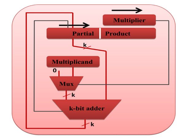 ).
).
 |
Fig. (1) Typical k-bit Sequential Multiplier. |
3.1. Carry Save Addition (CSA)
Addition algorithm is the most essential and frequent operation used in digital computer arithmetic. To reduce the time delay especially for large hardware design, faster methods to add binary numbers with least carry propagation delay are used such as the Carry Save Adder (CSA) which has the smallest carry propagation delay where n-bit carry-save adder take a delay time of one full adder for any n (i.e. the maximum delay for n × n bit multiplication will never exceed n full adder time delay).
CSA (high speed multi-operand adder) is also known as (3:2) counter [34M.D. Ercegovac, and T. Lang, Digital Arithmetic., Morgan Kaufmann Publishers, Elsevier: San Antonio, USA, vol. 1. 2004.] where the addends are three and the result is produced as two vectors. Fig. (2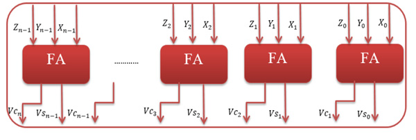 ) shows the internal architecture of N-bit CSA, it consists of n disjoint full adders (FAs) where each of which computes a single sum and carry bit based on the corresponding bits of the three input numbers. Unlike conventional adders, such as carry ripple adder, CSA consists of multiple one-bit full adders without any carry chaining. Such carry propagation free addition schemes will provide the results in a redundant form. The redundant results appear as sum vector (VS) and carry vector (VS) that can be described as in the following equations: S = (x + y + z)mod 2 & C = [(x + y + z) - s] / 2
 |
Fig. (2) Internal architecture of N-bit CSA. |
3.2. Carry Lookahead Adder (CLA)
Reducing the carry propagation delay of two-operand adders is a major factor in digital arithmetic field as most other arithmetic operations (such as multiplication and division) are implemented using several addition and subtraction iterations. Computer arithmetic researchers presented different logic design approaches to overcome the carry propagation problem. One commonly used solution is via the use of Carry Look-ahead Addition (CLA) which calculates the carry signals in advance based on the input signals [34M.D. Ercegovac, and T. Lang, Digital Arithmetic., Morgan Kaufmann Publishers, Elsevier: San Antonio, USA, vol. 1. 2004.].
The internal architecture of N-bit Carry Lookahead Adder (CLA) is shown in Fig. (3a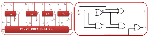 ). It consists of n Full Adders (FAs) where each of these deals with two input digits Xi and Yi along with the Ci signal compute three signals s: sum, g: generate and p: propagate. While Fig. (3b) shows internal signals of full adder used for CLA logic where Gi is the carry generate signal as a carry (Ci+1 ) is generated whenever Gi = 1 regardless of the input carry (Ci ). In addition,Pi is the carry propagate signal since whenever Pi = 1, the input carry is propagated to the output carry, i.e., Ci+1 = 1(i.e. note that whenever Pi = 1 and Gi = 1).
 |
Fig. (3) (a) Internal architecture of N-bit Carry Lookahead Adder (b) Full adder circuit. |
CLA logic uses the concepts of generating and propagating carries where adding two one-bit inputs x and y is said to generate in two cases: (a) if both bits Xi = 1 and Yi = 1 are 1 and (b) if either Xi = 1 and Yi = 1 is 1 and the Ci = 1 is 1. Computing the values of Pi = 1 and Gi = 1 only depends on the input operand bits (Ai = 1 and Bi = 1) as clear from the figure and the following equations. The propagate (P) , generates (G) in a full-adder, Sum (Si ) and Carry-Out (Ci+1) expressions are given as:
 |
For example: The Boolean expression of the Ci+1 of first 3-stages CLA can be derived as follows:
 |
4. HARDWARE IMPLEMENTATION AND SPECIFICATIONS
Constructing an efficient FPGA hardware coprocessor should consider several factors, such as the logic design techniques, components & interconnections, the hardware description language, the FPGA family kit, and the design simulation and synthesizing tools. The architecture of the proposed N-bit sequential multiplier is shown in Fig. (4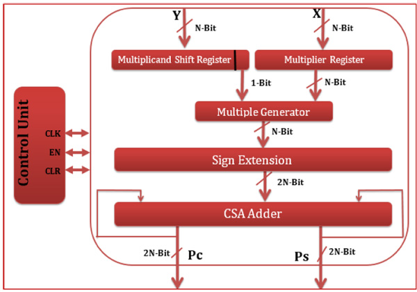 ). The design consists of two input operands (X and Y) with N-bit length, one output result in its final conventional form with N-bit length and three input control signals (Clock, Enable and Reset) as well as two control signals at the output (Acknowledgment and Ready).
According to Fig. (4), the proposed multiplier design is implemented mainly using two N-bit registers (a normal load register to hold the multiplier bits and shift register used to hold the multiplicand (Y) which performs 1-bit shift right with each clock cycle) and multiple generator circuit to generate partial products by performing AND operation between the LSB of Y and the whole vector of X, One 2N-bit register used for sign extension of each partial product register from N to 2N and one 2N-bit [3:2] CSA reduction adder to perform shift-and-add multiplication and the result of multiplication will be in redundant form with two vectors (Ps,Pc). To retrieve the final product result in a conventional form, we have implemented and examined an additional stage in two methods: one uses CLA adder and generates the final product with an expected delay time of
 |
Fig. (4) Internal architecture of N-bit Sequential Multiplier. |
 |
While the other uses CSA adder for two times which generates the final product with expected delay time of [K * CSAs]. The two methods final stage are shown in Fig. (5a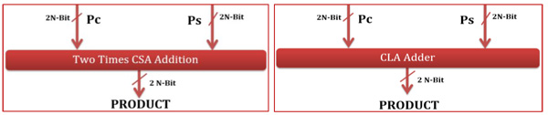 and b).
 |
Fig. (5) (a) Conventional product result using CSA (b) Conventional product result using CLA. |
The proposed implementation of sequential multiplier works as follows: Multiplication begins when enable and reset signal are activated (logic high) and the start pulse is issued, then the input registers will contain operands X and Y in one clock pulse. After accepting these data inputs, the multiplier begins its multiplication process and when it is completed, it starts sending the result out on the data bus. When Ps vector is placed on data bus, the ACK output signal is issued. When both vectors (Ps,Pc) are outputted, they become 1 and enable/reset goes low, and the multiplier is ready for another set of data. The summarized methodology of the proposed sequential multiplier design and the verification are shown in Fig. (6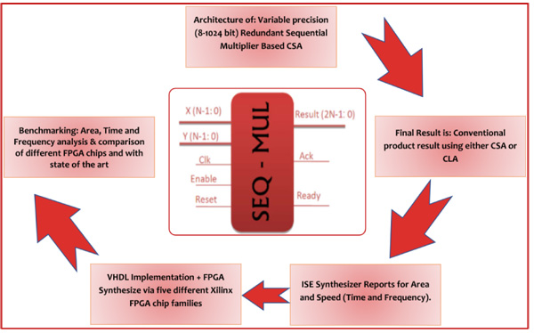 ).
).
 |
Fig. (6) Summary of work methodology of sequential multiplier design, testing and benchmarking.. |
The sequential multiplier design internally based on shift and add algorithm using CSA adder Fig. (4) has been implemented using VHDL (VHSIC Hardware Description Language, VHSIC is Very High Speed Integrated Circuit) with two methods for retrieving the final conventional product result Fig. (5) by either using CSA for two more times so that VC will be killed (i.e.VC = 0) and all bits will be included into VS (Final result = VS) it is called SQL_MUL_CSA or by using CLA as high speed two operand conventional adder, it is called SQL_MUL_CLA adder for different data-path sizes (8-, 16-, 32-, 64-, 128-, 256, 512-, 1024- bit), the simulation results were generated using Xilinx Synthesizer design suite version 14.2 tools, the target chip technology Xilinx kintex7 (device: xc7k480t, package: ffg1156, speed: -3). Also, for benchmarking purposes and comparison between different FPGA devices, we synthesized our proposed VHDL implementation for 1024 –bit data-path size for four more Xilinx FPGA kits; namely: vertix7 (xc7v2000t-2flg1925), artix7 (xc7a100t-3csg324), zynq7 (xc7z045-3ffg900) and Spartan 6 (xc6clx150t-4csg484). In addition, ModelSim-10.1d software package was used as simulation and verification tool and Maple worksheets soft 9.0 for mathematical verification purposes. Finally, the synthesizing and tests are performed with high performance multiprocessor computer platform (4th generation Intel Core I7 Quad-Core 3.4GHZ, 8MB shared cache with 16GB DDR3 - 1600MHZ).
5. RESULTS AND COMPARISONS
In this section, we present the various results collected from synthesizing reports of our VHDL code implementations were generated using Xilinx synthesizer ISE 14.2 tool. The delay time values used in following tables are calculated as the expected longest source clock period (from source rise to destination rise) multiplied by the number of logic stages (levels) required by the synthesizer to travel from input of a flip-flop or latch to travel through logic and routing and arrive at the output of the chip before the next clock edge including the clock-to-Q delay of the source flip-flop and the path delay from that flip-flop to the output pad [35 Available from https://forums.xilinx.com] as shown in the example in Fig. (7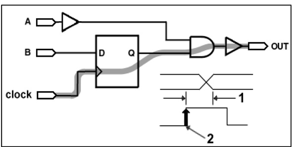 ), for example: the estimated total time delay (for 64 bits Seq_Mul_CSA) = Source Clock x 4 Logic Levels when synthesized using kintex7 chip (= 2.461 ns * 4 = 9.844 ns). The source clock period and the number of logic stages change with the change of data-path size (e.g. the number of levels for 1024 bit data path size and source clock period of similar chip and design coding is 11 stages and 3.381ns, respectively), the design coding (e.g. the number of levels for 64_Bit_Seq_Mul_CLA and source clock period for the same chip family are 7 stages and 4.369ns, respectively) and FPGA device (e.g. the number of levels for 1024 bit data path size will be changed from 11 stages to 12 stages as we change the chip device from (xc7k480t-3ffg1156) to (xc7k70t-3fbg676). While the maximum frequency was calculated as the reciprocal of minimum period of delay (already computed by synthesizer and affected by similar factors).
 |
Fig. (7) Source clock estimation [35 Available from https://forums.xilinx.com]. |
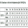
Table (1) along with the bar charts (a, b) in Fig. (8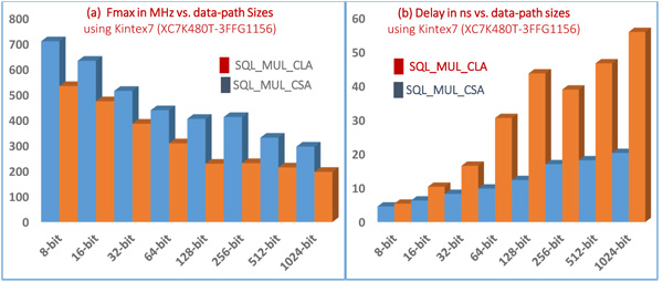 ) compared the maximum frequency values (in MHz) and the total delay time (in ns) of different design data-path sizes (32-, 64-, 128-, 256-, 512-, and 1024 bits) targeting kintex7-xc7k480t-3ffg1156 chip for both implementations Seq_Mul_CSA and Seq_Mul_CLA. Explicitly, Seq_Mul_CSA is normally faster than Seq_Mul_CLA for all bit lengths, therefore, we will focus our discussion on Seq_Mul_CSA leaving the results of Seq_Mul_CLA for benchmarking needed by other researchers. As clearly seen, the 8-bit multiplier has recorded the highest frequency (710.227 MHz) and lowest delay (4.572 ns) as it is considered the smallest data-path size. Such 8-bit multiplier might be used as a building block for larger multiplier circuits. Table (2) shows the amount of hardware utilization results for both multipliers represented in two hardware factors: the number of utilized registers (the total number of registers in the target device is 597200) and the number of utilized Lookup Tables - LUTs (the total number of LUTs in the target device is 298600). The maximum utilization was registered for 1024-bit multiplier with 17443 (2%), and 21538 (3%) registers as well as 7557 (2%) and 16677 (5%) LUTs for both Seq_Mul_CSA and Seq_Mul_CLA respectively with relatively increased hardware requirements for Seq_Mul_CLA of the design with all data-path sizes. To sum up, the design data-path size is directly proportional with the total delay time, inversely proportional maximum frequency values, and directly proportional to the number of registers and LUTs.
 |
Fig. (8) Multiplier precision (in bits) vs. (a) Maximum Frequency (MHz) (b) Total Delay (ns) for both implementations. |
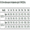
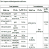
Table (3) along the bar charts (a, b) in Fig. (9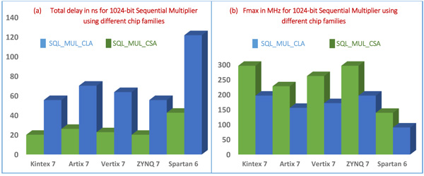 ) compared the maximum frequency and the total delay of proposed 1024-bit sequential multiplier designs implemented using different chip families (vertix7, kintex7, artix7, zynq7 and spartan6). The results showed that the design of 1024-bit Seq_Mul_CSA using kintex7 device is domineering the results in terms of maximum frequency with 296 MHz and approximate total delay time 20.3 ns while spartan6 device recorded the lowest frequency with 140 MHz and approximate total delay time 40 ns. Zynq7 device recorded similar values for the 1024-bit device (with lower numbers for smaller devices and less hardware resources). The next two devices have higher rates, the maximum frequency for design based vertix7 and artix7 is greater than spartan6 by almost 87% and 63% respectively. The performance evaluation results for the design of 1024-bit Seq_Mul_CLA showed similar tendency with much frequency numbers and higher total delay values.
 |
Fig. (9) Proposed 1024-bit sequential multipliers using different chip families (a) Maximum frequency (b) total Delay. |
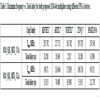
Even though some of the previous designs might be different in the design architecture, data-path size and devices technology, nevertheless the comparison between our proposed implementations with other designs can be valid as it showed that the proposed design is very competitive with many dedicated solutions. For instance, Table (4) summarizes the comparisons of the proposed design with different designs existed in the literature. The FPGA implementations of different 8-bit multipliers in [22A. Sharma, "FPGA Implementation of a High-Speed Multiplier Employing Carry Lookahead Adders in Reduction Phase", International Journal of Computer Applications, vol. 116, no. 17, ., 26K. Babulu, and G. Parasuram, "FPGA Realization of Radix-4 Booth Multiplication Algorithm for High Speed Arithmetic Logics", International Journal of Computer Science and Information Technologies, vol. 2, no. 5, pp. 2102-2107.-29M.C. Sudeep, S. Bimba, and M. Vucha, "Design and FPGA implementation of high speed Vedic multiplier", International Journal of Computer Applications, vol. 90, no. 16, .] recorded a total delay values of 29.4 ns, 5.22 ns, 24.6 ns, 5.6 ns and 15.7 ns, respectively which means that our proposed sequential CSA multiplier is approximately 6.4, 1.14, 5.4, 1.22, and 3.43 times faster, respectively.
Also, authors of [23S. Singh, and S. Mittal, "VHDL Design and Implementation for Optimum Delay & Area for Multiplier & Accumulator Unit by 32-Bit Sequential Multiplier", International Journal of Engineering Trends and Technology, vol. 3, no. 5, pp. 683-686.-25J. Rao, and S. Dubey, "A High-Speed Wallace Tree Multiplier Using Modified Booth Algorithm for Fast Arithmetic Circuits", Journal of Electronics and Communication Engineering, vol. 3, no. 1, pp. 7-11.
[http://dx.doi.org/10.9790/2834-0310711] ] proposed a 32-bit sequential multiplier, 32-bit booth multiplier, and 32-bit Wallace tree multiplier synthesized for Xis2 –chip, Spartan 3 and Vertix6 low power (xc6vlx75tl-1lff484), respectively and they reported a total delay times of 9.0 ns, 81.8 ns, and 9.536 ns. For our processor, it is 8.276 ns (515.31 MHz), therefore, our processor throughputs are 1.09, 9.9 and 1.15 times greater, respectively. Furthermore, we have compared our proposed multiplier with the 512-bit Montgomery multiplier proposed by V. Skobic, et.al., [30V. Škobic’, B. Dokic’, and E. Ivanovic’, "FPGA Implementation of Montgomery Modular Multiplier", 5th Small Systems Simulation Symposium, Serbia, .] who targeted the FPGA chip device Altera Cyclone IV (ep4ce115f29c7) and reported a maximum frequency of 239.8MHz which is slower than our multiplier by 91 MHz (27.5% slower).
Eventually, the proposed work in this paper generates many comparable synthesize results to design the sequential multiplication unit using parallel/redundant arithmetic processors especially those used commonly in cryptographic systems over a known finite field. It was found that choosing the best chip technology would increase the throughput of the arithmetic operations.
CONCLUSION
Multiplication is an essential building block for several digital processors as it requires a considerable amount of processing time and hardware resources. A fast FPGA implementation of sequential multiplication unit based on carry save addition via Xilinx kintex7 device technology that improves the computation process is proposed in this paper. The redundant result of proposed multiplier has been restored to its conventional format by applying CSA addition twice to end up with a result stored at the sum vector (so-called Seq_Mul_CSA) or by applying CLA which is a well-known fast two operand conventional adder (so-called Seq_Mul_CLA). The performance of both implementations was studied in terms of timing issues (maximum frequency and total time delay) and the hardware utilization of FPGA kit. The paper proofs the distinction of sequential multiplication with carry save over other multiplication techniques when implemented with kintex7 FPGA chip (via VHDL) as it computes the 1024 x 1024-bit multiplication with approximate delay 20.3 ns and maximum frequency of 296 MHz which is considered a very attractive and competent values.
CURRENT & FUTURE DEVELOPMENTS
A complete FPGA design architecture and VHDL coding implementation of sequential multiplier coprocessor based on CSA Addition using Xilinx FPGA chip families is introduced in detail in this paper. This research is substantial for many Cryptoprocessor and embedded system designers as many patented and non-patented researches are currently up-to-date to target the multiplication unit architectures, designs, circuits and implementations as well as synthesizing for programmable devices and large operands (data-path size). Future work of this research can focus on different issues, such as the sequential design-based sign digit addition, implementing large multipliers using smaller ones, using different radix system such as radix-4 with recording, analyzing the design with different design technology such as ASIC or Microprocessors, applying other multipliers methods using similar FPGA chips such as Karatsuba multiplier and others.
CONSENT FOR PUBLICATION
Not applicable.
CONFLICT OF INTEREST
The authors confirm that this article content has no conflict of interest.
ACKNOWLEDGEMENTS
Declared none.
REFERENCES
| [1] | E.D. Automation, "About the EDA Industry", Electronic Design Automation Consortium, 2015 http://www.edac.org |
| [2] | C. Maxfield, “The Design Warrior’s Guide to FPGAs: devices, tools and flows”, Mentor Graphics Corporation and Xilinx., Elsevier, 2004 |
| [3] | D.L. Perry, "VHDL: Programming by Example", 4th ed., the McGraw-Hill Companies, 2002 |
| [4] | K.H. Tan, and A. Wassal, "Galois field multiplier system and method", US Patent 8099655 B1, Jan 17, 2012 |
| [5] | Q. Abu Al-Haija, and A. Al Badawi, "Cost-effective design for binary Edwards elliptic curves crypto-processor over GF (2N) using parallel multipliers and architectures", International Journal of Information and Computer Security, Inderscience, vol. 5, no. 3, pp. 236-250. [http://dx.doi.org/10.1504/IJICS.2013.055840] |
| [6] | R. Goyal, A.K. Dey, and N. Gupta, "Binary adder and multiplier circuit", US Patent 8933731 B2, Jan 13, 2015 |
| [7] | M. Langhammer, and K. Tharmalingam, "Large multiplier for programmable logic device", US Patent 8788562 B2, Jul 22, 2014 |
| [8] | M.M. Kamble, and S.P. Ugale, "Analysis of different multiplication algorithm and FPGA implementation of recursive barrel shifter method for multiplication", International Research Journal of Engineering and Technology, vol. 3, no. 1, pp. 1141-1142. |
| [9] | M. Rakesh, and P.S. Rani, "Design and Implementation of High Speed 64-bit VEDIC Multiplier", International Journal of Emerging Research in Management &Technology, vol. 5, no. 5, . |
| [10] | S. Thawait, and J. Verma, "FPGA Implementation of Simple and High-Speed Vedic Multiplier", SSRG International Journal of VLSI & Signal Processing, vol. 2, no. 3, . |
| [11] | S. Tamilselvan, "Design, Analysis and FPGA Implementation of N Bit Vedic Multiplier Based on Different Adder Architectures", International Journal of Advanced Research in Computer and Communication Engineering, vol. 4, no. 8, pp. 72-76. |
| [12] | H. Mohammed, and Al Mijalli, "Spartan-3A FPGA Implementation", World Applied Sciences Journal, vol. 18, no. 9, pp. 1291-1295. |
| [13] | V.R. Raut, and P.R. Loya, "FPGA Implementation of Low Power Booth Multiplier Using Radix-4 Algorithm", International Journal of Advanced Research in Electrical, Electronics and Instrumentation Engineering, vol. 3, no. 8, . [http://dx.doi.org/10.15662/ijareeie.2014.0308081] |
| [14] | R. Pradhisha, "FPGA Implementation of Self-Testing Logic gates, Adders and Multipliers", Indian Journal of Science and Technology, vol. 8, no. 22, pp. 23263-23271. [http://dx.doi.org/10.17485/ijst/2015/v8i22/79331] |
| [15] | V. Satya Kishore, J.E. Abhilash, and G.N. Ratnakishor, "FPGA Implementation & Performance Comparison of Various High Speed Unsigned Binary Multipliers using VHDL", International Journal on Recent and Innovation Trends in Computing and Communication, vol. 2, no. 12, . |
| [16] | V. Kunchigi, L. Kulkarni, and S. Kulkarni, "High Speed and Area Efficient Vedic Multiplier", International Conference on Devices, Circuits and Systems (ICDCS), pp. 360-364. [http://dx.doi.org/10.1109/ICDCSyst.2012.6188747] |
| [17] | S. Khatri, and G. Jangid, "FPGA Implementation of 64-bit fast multiplier using barrel shifter", International Journal for Research in Applied Science and Engineering Technology, vol. 2, no. 7, pp. 86-95. |
| [18] | D.J. Udhani, and R.C. Patel, "Implementation of high speed multiplier on FPGA", International Journal of Science, Engineering and Technology Research, vol. 3, no. 2, . |
| [19] | S. Kaur, and P.S. Jassal, "FPGA Implementation of Double Precision Floating Point Multiplier using Xilinx Coregen Tool", International Journal of Electronics and Computer Science Engineering, vol. 2, no. 3, . |
| [20] | M. Issad, B. Boudraa, M. Anane, and S. Seddiki, "FPGA Implementation of Modular exponentiation using single modular multiplier", 2014 International Conference on Circuits, Systems, Signal Processing, Communications and Computers (CSSCC ’14), pp. 162-167. |
| [21] | P. Agrawal, and R. Sinha, "Comparative Analysis and FPGA Implementation of Vedic Multiplier for various Bit Lengths using Different Adders", International Journal of Innovative Research in Computer and Communication Engineering, vol. 3, no. 10, p. 29. |
| [22] | A. Sharma, "FPGA Implementation of a High-Speed Multiplier Employing Carry Lookahead Adders in Reduction Phase", International Journal of Computer Applications, vol. 116, no. 17, . |
| [23] | S. Singh, and S. Mittal, "VHDL Design and Implementation for Optimum Delay & Area for Multiplier & Accumulator Unit by 32-Bit Sequential Multiplier", International Journal of Engineering Trends and Technology, vol. 3, no. 5, pp. 683-686. |
| [24] | M. Chaudhary, and M.S. Narula, "FPGA Implementation of Booth’s and Baugh- Wooley Multiplier Using Verilog", International Journal of Innovative Technology and Exploring Engineering, vol. 3, no. 1, pp. 2278-3075. |
| [25] | J. Rao, and S. Dubey, "A High-Speed Wallace Tree Multiplier Using Modified Booth Algorithm for Fast Arithmetic Circuits", Journal of Electronics and Communication Engineering, vol. 3, no. 1, pp. 7-11. [http://dx.doi.org/10.9790/2834-0310711] |
| [26] | K. Babulu, and G. Parasuram, "FPGA Realization of Radix-4 Booth Multiplication Algorithm for High Speed Arithmetic Logics", International Journal of Computer Science and Information Technologies, vol. 2, no. 5, pp. 2102-2107. |
| [27] | M. Thomas, "Design and Simulation of Radix-8 Booth Encoder Multiplier for Signed and Unsigned Numbers", International Journal for Innovative Research in Science & Technology, vol. 1, no. 1, pp. 2349-6010. |
| [28] | "FPGA Implementation of 8-bit multiplier with reduced delay time", International Journal of Computer and Communication Engineering, vol. 2, no. 6, p. 665. |
| [29] | M.C. Sudeep, S. Bimba, and M. Vucha, "Design and FPGA implementation of high speed Vedic multiplier", International Journal of Computer Applications, vol. 90, no. 16, . |
| [30] | V. Škobic’, B. Dokic’, and E. Ivanovic’, "FPGA Implementation of Montgomery Modular Multiplier", 5th Small Systems Simulation Symposium, Serbia, . |
| [31] | A. Kareem, M. Vardhana, and P. Kumar, "VLSI Implementation of High Speed-Low Power-Area Efficient Multiplier Using Modified Vedic Mathematical Techniques", Recent Patents on Computer Science, vol. 9, no. 3, pp. 216-221. [http://dx.doi.org/10.2174/2213275908666150220203501] |
| [32] | Available from https://www.xilinx.com/products/silicon-devices/fpga.html |
| [33] | A. Saado, "Canonical signed digit (CSD) coefficient multiplier with optimization",US Patent 7680872 B2, Mar 16, 2010 |
| [34] | M.D. Ercegovac, and T. Lang, Digital Arithmetic., Morgan Kaufmann Publishers, Elsevier: San Antonio, USA, vol. 1. 2004. |
| [35] | Available from https://forums.xilinx.com |