- Home
- About Journals
-
Information for Authors/ReviewersEditorial Policies
Publication Fee
Publication Cycle - Process Flowchart
Online Manuscript Submission and Tracking System
Publishing Ethics and Rectitude
Authorship
Author Benefits
Reviewer Guidelines
Guest Editor Guidelines
Peer Review Workflow
Quick Track Option
Copyediting Services
Bentham Open Membership
Bentham Open Advisory Board
Archiving Policies
Fabricating and Stating False Information
Post Publication Discussions and Corrections
Editorial Management
Advertise With Us
Funding Agencies
Rate List
Kudos
General FAQs
Special Fee Waivers and Discounts
- Contact
- Help
- About Us
- Search


The Open Electrical & Electronic Engineering Journal
(Discontinued)
ISSN: 1874-1290 ― Volume 13, 2019
On the Use of 6th-Order Tunable Complementary Metal-Oxide-Semiconductor Varactor based Filter in Ultra-Wideband Low Noise Amplifier
Farooq Khaleel, M. Nadhim Abbas*
Abstract
Background:
The plethora of the emerged radio frequency applications makes the frequency spectrum crowded by many applications and hence the ability to detect specific application’s frequency without distortion is a difficult task to achieve.
Objective:
The goal is to achieve a method to mitigate the highest interferer power in the frequency spectrum in order to eliminate the distortion.
Method:
This paper presents the application of the proposed tunable 6th-order notch filter on Ultra-Wideband (UWB) Complementary Metal-Oxide-Semiconductor (CMOS) Low Noise Amplifier (LNA) utilising self-forward body bias (SFBB).
Results:
The proposed filter presents 23.5dBm minimum interferer rejection (IR) and attenuates the interferer signal from -43dBm to -67dBm at frequency 5.17GHz. In addition, the maximum IR is 40dBm and attenuates the interferer signal from -41dBm to -81dBm at frequency 5.785GHz. The proposed filter provides coarse tuning with frequency spacing (10MHz) and soft tuning with frequency spacing (1MHz). The UWB CMOS LNA consumes only 5.22mW from a supply voltage of 1.2V and presents a maximum gain of 14dB at frequency 6.25GHz in the -3dB bandwidth from 4.75GHz to 7.5GHz. In addition, the average noise figure is 3.1dB and the input insertion losses (S11) is less than -12dB along the designed bandwidth. The simulation is performed in Advanced Design System (ADS2016.01) software utilising 180nm Taiwan Semiconductor Manufacturing Company (TSMC) Berkeley Short-channel Insulated Gate Field Effect Model (BSIM3v3) model files.
Conclusion:
The proposed method achieves high interferer power rejection with both soft and coarse tuning.
Article Information

Identifiers and Pagination:
Year: 2018Volume: 12
First Page: 21
Last Page: 33
Publisher Id: TOEEJ-12-21
DOI: 10.2174/1874129001812010021
Article History:
Received Date: 12/1/2018Revision Received Date: 03/4/2018
Acceptance Date: 10/5/2018
Electronic publication date: 31/05/2018
Collection year: 2018
open-access license: This is an open access article distributed under the terms of the Creative Commons Attribution 4.0 International Public License (CC-BY 4.0), a copy of which is available at: https://creativecommons.org/licenses/by/4.0/legalcode. This license permits unrestricted use, distribution, and reproduction in any medium, provided the original author and source are credited.
* Address correspondence to this author at the Department of Electrical Engineering, University of Baghdad, Jadriya, Baghdad, Iraq; Tel: +9647712343590; E-mail: mohammed.nadhim@uob.edu.iq
| Open Peer Review Details | |||
|---|---|---|---|
| Manuscript submitted on 12-1-2018 |
Original Manuscript | On the Use of 6th-Order Tunable Complementary Metal-Oxide-Semiconductor Varactor based Filter in Ultra-Wideband Low Noise Amplifier | |
1. INTRODUCTION
The C-band microwave frequency designation is fully occupied by multiple applications and multiple channels for each application, for example, the 802.11a 5GHz, UWB, WiMAX 802.16e standards [1H. Zhang, S. Member, E. Sánchez-sinencio, L. Fellow, and I. Paper, "Linearization Techniques for CMOS Low Noise Amplifiers: A Tutorial", vol. 58, no. 1, pp. 22–36, 2011.]. The plethora of these emerged services and their channels causes two or more nearby signals to enter the receiver simultaneously and consequently distorts the desired signal. The nearby signals necessitate the use of very sharp cutoff frequency-response filter to considerably mitigate the high power of the interferer signal and, as a result, allows only the desired signal to enter the receiver chain [2T-K. Nguyen, N-J. Oh, C-Y. Cha, Y-H. Oh, G-J. Ihm, and S-G. Lee, "Image-rejection CMOS Low-Noise Amplifier Design Optimization Techniques", IEEE Trans. Microw. Theory Tech., vol. 53, no. 2, pp. 538-547.
[http://dx.doi.org/10.1109/TMTT.2004.840744] ].
The third-order notch filter –a type of sharp cutoff frequency filter was described in details, for the first time, for 5GHz, 240nm CMOS Wireless LAN receiver front end [3H. Samavati, H.R. Rategh, and T.H. Lee, "A 5-GHz CMOS wireless LAN receiver front end", IEEE J. Solid-State Circuits, vol. 35, no. 5, pp. 765-772.
[http://dx.doi.org/10.1109/4.841505] ]. The use of both, the proposed third-order notch filter applied to the LNA stage and an image-reject Phase-Locked Loop (PLL), attenuated the image signal. However, if the RF input signal, for example, was at 5.2GHz, then the image signal would lie at 4.6GHz. This would have resulted in a frequency spacing of 600MHz between the desired signal and the image signal. The aforementioned frequency spacing is large and does not require sharp cutoff frequency filter. In addition, the filter attenuated the image signal by only 12dB and the RF input signals were limited in the range from 5.15GHz to 5.35GHz, which did not cover all the 5GHz band channels. The LNA achieved a high-value noise figure (NF) for busy channels (4.8dB). Moreover, the LNA stage consumed a relatively high value for low power applications requirements (7.2mW). Although the LNA differential topology attenuated the on-chip interferences much better than other LNA topologies, it took a large area.
The same third-order notch filter presented in [3H. Samavati, H.R. Rategh, and T.H. Lee, "A 5-GHz CMOS wireless LAN receiver front end", IEEE J. Solid-State Circuits, vol. 35, no. 5, pp. 765-772.
[http://dx.doi.org/10.1109/4.841505] ] was optimised to mitigate the image signal located at 4.25GHz for 5.25GHz, 180nm CMOS Wireless Local Area Networks (WLAN) receivers [2T-K. Nguyen, N-J. Oh, C-Y. Cha, Y-H. Oh, G-J. Ihm, and S-G. Lee, "Image-rejection CMOS Low-Noise Amplifier Design Optimization Techniques", IEEE Trans. Microw. Theory Tech., vol. 53, no. 2, pp. 538-547.
[http://dx.doi.org/10.1109/TMTT.2004.840744] ]. The good gain (20.5dB) achieved was hampered by high power consumption (12mW)—a major issue for low power RF applications. Moreover, the difference between the wanted and image signals was 1GHz, therefore, it did not need sharp cutoff frequency filter. In addition, the filter attenuated fixed image frequency at 4.25GHz and it did not tune to attenuate interferers, which might appear near the desired signal if many transmitters occupied the channel spectrum.
An active inductor was proposed and simulated to tune the image rejection frequency for the same filter proposed in [3H. Samavati, H.R. Rategh, and T.H. Lee, "A 5-GHz CMOS wireless LAN receiver front end", IEEE J. Solid-State Circuits, vol. 35, no. 5, pp. 765-772.
[http://dx.doi.org/10.1109/4.841505] ]. However, the simulation data [4L.C. Lee, A.K.b. A’ain, and A.V. Kordesch, "A 5 GHz CMOS Tunable Image-Rejection Low-Noise Amplifier", in 2006 International RF and Microwave Conference, 2006, pp. 152–156.] for the proposed 5GHz, 180nm CMOS LNA resulted in a very large power consumption (15.46mW) due to the LNA topology used. The frequency spacing between the wanted signal and image signal was also large (850MHz); therefore, it did not need very sharp cutoff frequency filter to attenuate the image signal.
The same authors in [4L.C. Lee, A.K.b. A’ain, and A.V. Kordesch, "A 5 GHz CMOS Tunable Image-Rejection Low-Noise Amplifier", in 2006 International RF and Microwave Conference, 2006, pp. 152–156.] simulated a 2.4GHz, 180nm CMOS LNA with the same IR filter presented in [3H. Samavati, H.R. Rategh, and T.H. Lee, "A 5-GHz CMOS wireless LAN receiver front end", IEEE J. Solid-State Circuits, vol. 35, no. 5, pp. 765-772.
[http://dx.doi.org/10.1109/4.841505] ] and [4L.C. Lee, A.K.b. A’ain, and A.V. Kordesch, "A 5 GHz CMOS Tunable Image-Rejection Low-Noise Amplifier", in 2006 International RF and Microwave Conference, 2006, pp. 152–156.]. However, the tuning range in [5L.C. Lee, A.K.b. A’ain, and A.V. Kordesch, "A 2.4-GHz CMOS Tunable Image-Rejection Low-Noise Amplifier with Active Inductor", in APCCAS 2006 - 2006 IEEE Asia Pacific Conference on Circuits and Systems, 2006, pp. 1679–1682.
[http://dx.doi.org/10.1109/APCCAS.2006.342107] ] was only 400MHz from 1.08GHz to 1.41GHz. The frequency spacing between the desired and interferer signal was over 1GHz. As a result, the filter sharpness was not again a major issue. In addition, the simulation data presented very high power consumption of 20mW due to the LNA topology used.
Many RF applications utilised the capacitance of the MOSFET as a tuning element. For example, the 110nm CMOS VCO utilised the capacitance slope change of the accumulation mode MOS varactor to vary the gain [6Y. Liu, "Reliability analysis of MOS varactor in CMOS LC VCO", Microelectronics J., vol. 42, no. 2, pp. 330-333.
[http://dx.doi.org/10.1016/j.mejo.2010.12.003] ]. Another example, the MOS varactor was used in 250nm CMOS VCO to obtain wide tuning range of 500MHz [7A. Iji, X. Zhu, and M. Heimlich, "A 3GHz low power, MOS varactor voltage controlled oscillator for implantable ultra wideband applications in CMOS Silicon-On-Sapphire (SOS) process", in 2013 IEEE International Conference on Ultra-Wideband (ICUWB), pp. 278-281.
[http://dx.doi.org/10.1109/ICUWB.2013.6663862] ].
Our paper achieves the mitigation of the high power interferer signal that is considered very close to the desired signal. In addition, the mitigation of any high power interferer signal in the application’s frequency spectrum is possible. In addition, our paper proposes the use of PMOS varactor bank to tune the interferer rejection frequency within a frequency spacing of the only 10MHz away from the desired signal. This very low-frequency spacing requires the proposed 6th-order notch filter that provides very sharp cutoff frequency filter. The proposed filter assures enough gain attenuation for the interferer signal as well as high gain to amplify the desired signal. Moreover, the location of the desired signal and interferer signal has very close frequency spacing. The 5GHz 802.11a CISCO standard channel allocations are used as an example to demonstrate the proposed work [8C.I.S.C.O. Systems, "Radio Channel Frequencies", CISCO Systems, 2008.]. The proposed PMOS varactor bank is used, for the first time, in the suggested 6th-order notch filter to tune the interferer rejection frequency with maximum attenuation and much-closed frequency spacing. To reduce the high power consumption for the previously reported papers, the proposed IR filter is applied to the 180nm UWB CMOS LNA topology utilising SFBB technique described in [9C.M. Li, M.T. Li, K.C. He, and J.H. Tarng, "A Low-Power Self-Forward-Body-Bias CMOS LNA for 3-6.5-GHz UWB Receivers", IEEE Microw. Wirel. Compon. Lett., vol. 20, no. 2, pp. 100-102.
[http://dx.doi.org/10.1109/LMWC.2009.2038526] ].
2. MATERIALS AND METHODS
2.1. 6th-Order Passive Notch-Filter Design Technique
Two stages of the 3rd-order passive notch filter described in [3H. Samavati, H.R. Rategh, and T.H. Lee, "A 5-GHz CMOS wireless LAN receiver front end", IEEE J. Solid-State Circuits, vol. 35, no. 5, pp. 765-772.
[http://dx.doi.org/10.1109/4.841505] ] are cascaded to provide more poles and zeros resulting in more attenuation and sharpness response at the required rejection frequency. The proposed filter is shown in Fig. (1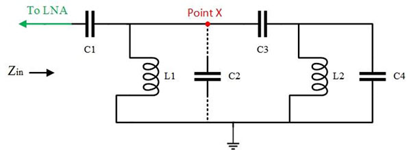 ).
).
 |
Fig. (1) 6th-Order Passive Notch Filter. |
The input impedance of the filter can be derived through parallel-serial impedance algebraic calculations to obtain the input impedance expression shown in Equation (1).
 |
(1) |
The zeros and poles terms from Equation (1) can be mathematically reduced to Equations (2) and (3), respectively.
 |
(2) |
Where,
x1 = (L1(C1 + C2 + C3)) + (L2(C3 + C4)) and α1 = (L1L2 (C3C4 + C2(C3 + C4) + C1(C3 + C4)))
 |
(3) |
Where,
x2 = (L1(C3 + C4)) + (L2(C2 + C3)) and α2 = (L1L2 ((C3C4) + (C2(C3 + C4))))
The filter components (C1, L1, C3, L2, C4, and C2) controls the rejection and passing frequencies according to the required design. However, the filter components values for C1, L1, C3, L2, and C4 are optimized to 24fF, 695pH, 1.2pF, 876pH, and 10pF, respectively, to guarantee sharp and high rejection value filter response. The optimization is done through the ADS quasi-newton optimization tool to get the suitable values for the filter’s components. In addition, the capacitor C2 is replaced by the PMOS varactor bank discussed in Section (B) to provide tunable interferer frequency rejection within very close frequency spacing and maintain the high interferer rejection value.
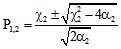
The input impedance could be further simplified to Equation (4). Fig. (2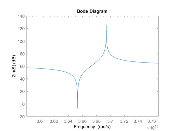 ) shows the sharp variation of the input impedance against frequency change in the working bandwidth.
 |
(4) |
Fig. (2) shows that the input impedance of the filter reduces to a very low value (acts as a short circuit to ground) at the desired rejection frequency. Consequently, the filter sinks the drain current and thus the signal is highly attenuated to pass through the following stages. For other frequency values rather than the rejection frequency, the filter acts as an open circuit allowing the signal to pass through the following stages.
 |
Fig. (2) Proposed Filter Input Impedance |
The filter transfer function can be derived as shown in Equation (5). In addition, the transfer function bode plot shows the sharpness of the proposed filter as shown in Fig. (3 ).
).
 |
Fig. (3) Proposed Filter Bode Plot. |
 |
(5) |
2.2. PMOS Varactor Bank Design Technique
In general, the passive capacitor value does not change with the applied voltage on the capacitor’s terminals. However, if the drain, source, and bulk terminals of the MOS device are connected together then the MOS gate capacitance value changes as the gate voltage varies because of the variation in charge concentration within the well and oxide interface. The aforementioned modification in MOS terminals’ connection results in a device called varactor, which can be considered as a voltage-controlled capacitor.
Fig. (4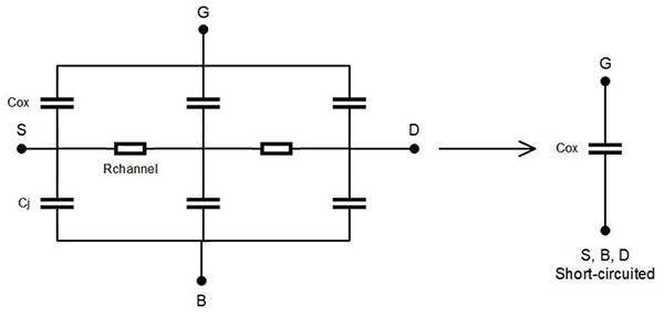 ) shows the small-signal equivalent circuit for the MOSFET, which has the source, drain, and bulk terminals are short-circuited, operating in accumulation mode [10R. Jacob Baker, CMOS Circuit Design, Layout, and Simulation., 3rd edJohn Wiley & Sons, Inc., .
[http://dx.doi.org/10.1002/9780470891179] ].
 |
Fig. (4) MOSFET small-signal equivalent circuit operating in accumulation mode. |
The junction capacitance (large value) is in series with the oxide capacitance (small value). The junction capacitance relation with the applied voltage is given as in Equation (6) [11T.H. Lee, The Design of CMOS Radio-Frequency Integrated Circuits., 2nd edCambridge University Press, .].
 |
(6) |
Where Cjo is the incremental capacitance at zero-bias, VF is the applied voltage across the junction, ɸ is the built-in voltage, and n is a variable that is related to doping profile. The junction capacitance is in series with the oxide capacitance and consequently, the total capacitance is approximately equal to the oxide capacitance.
Fig. (5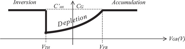 ) shows the variation of the PMOS gate capacitance versus the applied gate-bulk voltage along different PMOS operation modes.
 |
Fig. (5) PMOS gate capacitance variations versus gate-bulk voltage. |
By the aforementioned varactor connection and when operating in the accumulation mode, the varactor equivalent capacitance is constant and can be calculated as follows:
C’ox represents the oxide capacitance (εox/tox), where εox is the oxide permittivity and tox is the oxide thickness. The total gate capacitance is (C’ox*gate area), where the gate area is the multiplication of the gate width and gate length.
For the used 180nm TSMC process, consider, for example, the PMOS width is selected to be 13.2μm and the PMOS is operating in accumulation mode with a gate voltage of 3.3V, then the maximum capacitance that can be obtained is 20fF. The resultant maximum capacitance is relatively small value and subsequently the tuning of single PMOS varactor by varying the gate voltage results-in very small capacitances values that do not change the required cutoff frequency considerably. Therefore, a PMOS varactor bank consists of 30 PMOS varactors connected in parallel is proposed as shown in Fig. (6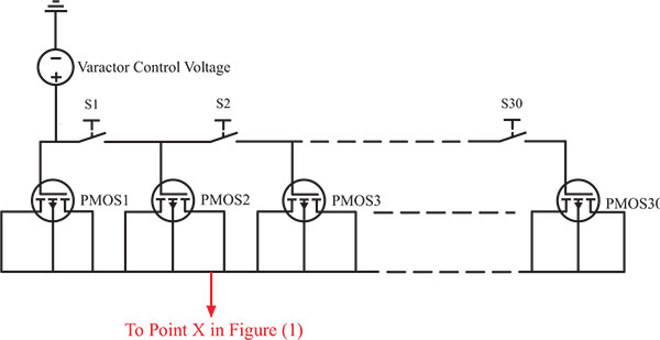 ).
).
 |
Fig. (6) Proposed PMOS varactor bank. |
The capacitor C2 in Fig. (1) is replaced by the proposed PMOS varactor bank, which allows the tuning of the designed rejection frequency by closing up the switches to increase the total capacitance that appeared at point X and thus changes the zeros locations in Equation (2). The interferer rejection frequency is reduced as more capacitors are connected in parallel to PMOS1 by closing the switches from 1 to 30.
Each PMOS varactor in the proposed varactor bank has a unique width optimised for the desired rejection frequency. Consequently, closing each switch will move the interferer rejection frequency with small frequency spacing (10MHz or more according to the required frequency) to the desired rejection frequency. This results in strong attenuation for the unwanted interferer frequency component in the frequency spectrum.
Furthermore, the varactor control voltage is used to provide soft tuning around the required rejection frequency with frequency steps of the only 1MHz. The tuning range provided by the varactor control voltage extends as more varactors connected in parallel because the highest peak of Cox is increased, for example, if one varactor is connected then the highest peak of Cox is lower than if all varactors are connected as shown in Fig. (4). Lower values of Cox provide less tuning range than higher Cox value as shown in Equation (2).
Fig. (7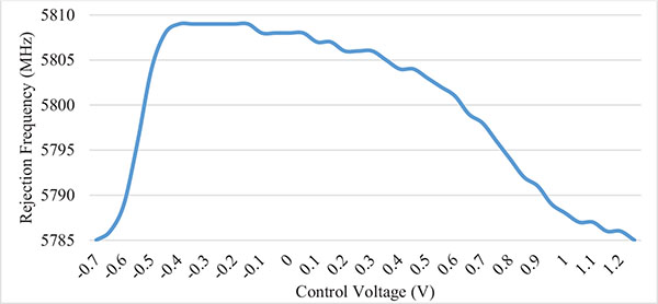 ) shows the tuning effect of the varactor control voltage on the rejected frequency location. The small tuning of control voltage provides 1MHz rejection frequency shifting above the 5785MHz. However, the shifting in the interferer rejection frequency reaches a maximum frequency of 5809MHz at a varactor control voltage of -0.25V providing only 24MHz tuning range above the frequency of 5785MHz.
 |
Fig. (7) Varactor control voltage tuning range for single connected varactor. |
On the other hand, if all varactors are connected then the rejection frequency could reach 5349MHz when the varactor control voltage is tuned to -0.35V providing 180MHz rejection frequency tuning range above the rejection frequency of 5169MHz as shown in Fig. (8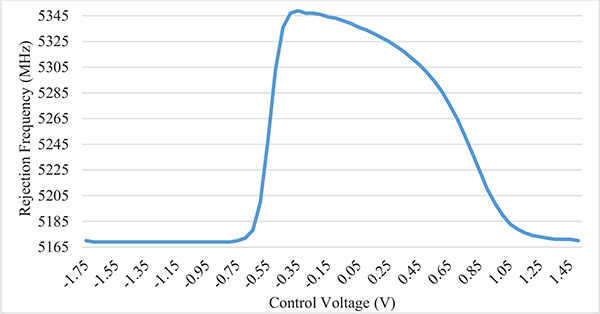 ).
).
 |
Fig. (8) Varactor control voltage tuning range when all varactors are connected. |
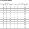
The designed PMOS varactor bank parameters are listed in Table 1, where the frequencies listed are for the CISCO IEEE802.11a standard channels.
2.3. Proposed PMOS Frequency Bank Application to UWB CMOS LNA
The previously design methodologies explained in Sections (A) and (B) are applied to the UWB CMOS LNA topology described by [9C.M. Li, M.T. Li, K.C. He, and J.H. Tarng, "A Low-Power Self-Forward-Body-Bias CMOS LNA for 3-6.5-GHz UWB Receivers", IEEE Microw. Wirel. Compon. Lett., vol. 20, no. 2, pp. 100-102.
[http://dx.doi.org/10.1109/LMWC.2009.2038526] ] in order to achieve low power consumption due to the suggested self-forward body biasing method, a high gain due to cascading two LNA amplifier stages, and good noise performance. The proposed filter is applied to the LNA’s second stage at the node between the common-source (Q3) and common-gate (Q4) amplifiers.
From Equations (1) and (2), the input impedance of the filter is at a minimum value-approaching zero at the desired interferer frequency. Consequently, the filter sinks the entire current between the common-source (Q3) and common-gate (Q4) stages. At any other frequencies, the filter impedance is high and the current will pass through the following stages. The proposed design methodology provides sharp cutoff response and very small frequency tuning (10MHz) because of the high order of the filter and the proposed PMOS varactor bank, respectively. In order to assemble the complete LNA schematic, the green arrow in Fig. (1) is connected to the green arrow in the main LNA topology schematic shown in Fig. (9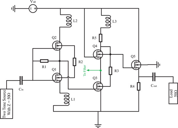 ), moreover, the red arrow in Fig. (6) is connected to the redpoint x node in Fig. (1). Table 2 summarizes the main LNA topology component values.
 |
Fig. (9) Main LNA Topology. |
3. SIMULATION RESULTS AND DISCUSSIONS
Many IEEE802.11a transmitters employed in a single geographic region lead to severe interference. Consequently, the CISCO IEEE802.11a standard frequency channels are taken as the input frequencies to the LNA. The design methodology described in Section (II) attenuates the highest power interferer that exists in the frequency spectrum. To verify the described design methodology, a two-tone source is connected to the LNA input. The two-tone inputs specify two input frequencies with an input power of -50dBm. The switches in the PMOS varactor bank can be controlled to change the required rejection frequency as shown in Table 1. The proposed filter achieves 23.5dBm minimum interferer rejection and attenuates the interferer signal from -43dBm to -67dBm at frequency 5.17GHz. In addition, the maximum IR is 40dBm and attenuates the interferer signal from -41dBm to -81dBm at frequency 5.785GHz. The gain (S21) attenuation at the interferer signal along the designed bandwidth is shown in Fig. (10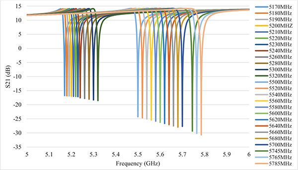 ). The varactor control voltage controls the working region of the PMOS varactor bank in the designed bandwidth.
 |
Fig. (10) Simulated S21 of the LNA. |
The average minimum noise figure in the operating bandwidth (4.75GHz-7.5GHz) is 3.1dB, neglecting the sharp peak that occurs at the interferer rejection frequency, as shown in Fig. (11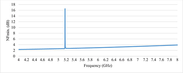 ).
).
 |
Fig. (11) Simulated NF of the LNA. |
The total filter’s inductors’ noise current justifies the sharp peak of noise that occurs at the interferer rejection frequency shown in Fig. (11). However, this noise’s sharp peak is settled quickly to the total LNA noise figure due to the filter sharpness. The proposed filter’s noise model is shown in Fig. (12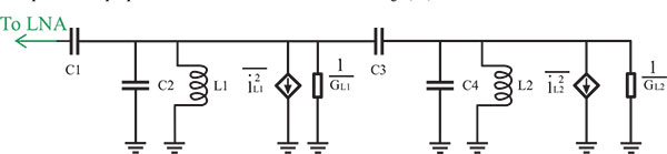 ).
).
 |
Fig. (12) Proposed Filter's Noise Model. |
When the filter is tuned to a certain interferer frequency, the filter input impedance is at its lower values, as shown in Fig. (2), that the filter is sinking the Q3 drain current. This results in high current values passing through the filter. Therefore, the noise current of the filter’s inductors is at maximum values leading to the sharp peak of noise. The total inductors’ current contribution to the total LNA noise current can be written as:
 = 4kT(GL1 + GL2), where
GLx = QLx*Lx*ωo,
ωo represents the rejection frequency,
x refers to the first and second filter’s inductors, and
QLx represents the inductors’ quality factor.
The LNA gain at the interferer and desired frequencies is investigated in terms of temperature variation as shown in Fig. (13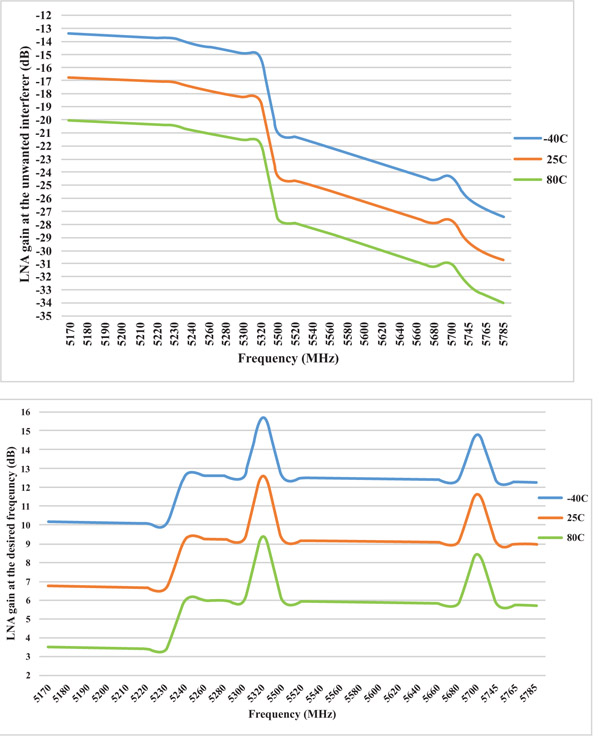 ).
).
 |
Fig. (13a) LNA gain at the rejected interferer with temperature variations. |
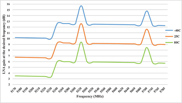 |
Fig. (13b) LNA gain at the desired signal with temperature variations. |
Fig. (13) show humps in the frequency response because of the variation of the filter’s total impedance at each different interferer frequency. The suggested varactor bank consists of reliable sizes for PMOS varactors and the humps in the frequency response can be avoided by selecting another width sizes for PMOS varactors, however, the new values can be practically impossible to implement.
The input and output return losses for the LNA are below (-12dB) in the working bandwidth providing input and output matching, respectively, as shown in Fig. (14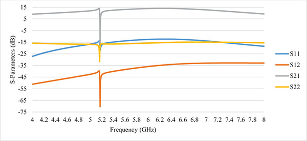 ).
).
 |
Fig. (14) Simulated S-Parameters of the LNA. |
Fig. (14) shows that the proposed PMOS bank filter provides a sharp response, that is, if the interferer signal is at 5.768GHz and the desired signal is at 5.785GHz, then the interferer signal is attenuated by -30.15dB and the desired signal is amplified by 9dB. Consequently, the difference between the two gains is 40dB in a frequency spacing of only 20MHz. In comparison, if the interferer signal is at 5.170GHz and the desired signal is at 5.18GHz, then the interferer signal is attenuated by -17dB and the desired signal is amplified by 7dB. Thus, the difference between the two gains is 24dB in a frequency spacing of only 10MHz.
The linearity of the suggested LNA is tested by two-tone test with two interferers having the power of -50dBm and a frequency spacing of 10MHz with centre frequencies 4.775GHz, 6GHz, and 7.4GHz, respectively, to cover the entire working bandwidth. The resultant IIP3 values are -12.8dBm, -13.75dBm, and -11.11dBm, respectively.
In addition, the LNA performance in comparison with other relevant and recent suggested LNAs is summarized in Table 3.
CONCLUSION
A variable 6th-order notch filter applied to low power UWB CMOS LNA topology has been demonstrated in ADS software utilising 180nm TSMC BSIM3v3 model files. The proposed work achieves sharp cutoff frequency behaviour and very small frequency tuning spacing. The minimum/maximum interferer rejection are 23.5/40dBm, respectively, with tunable interferer rejection range from 5.17GHz to 5.785GHz dedicated for the channels of IEEE802.11a standard receivers without changing the receiver’s performance. In summary, this work provides strong rejection for the interferers exist in the 5.8GHz band channels in IEEE802.11a receivers.
CONSENT FOR PUBLICATION
Not applicable.
CONFLICT OF INTEREST
The authors declare no conflict of interest, financial or otherwise.
ACKNOWLEDGEMENTS
Decleared none.
REFERENCES
| [1] | H. Zhang, S. Member, E. Sánchez-sinencio, L. Fellow, and I. Paper, "Linearization Techniques for CMOS Low Noise Amplifiers: A Tutorial", vol. 58, no. 1, pp. 22–36, 2011. |
| [2] | T-K. Nguyen, N-J. Oh, C-Y. Cha, Y-H. Oh, G-J. Ihm, and S-G. Lee, "Image-rejection CMOS Low-Noise Amplifier Design Optimization Techniques", IEEE Trans. Microw. Theory Tech., vol. 53, no. 2, pp. 538-547. [http://dx.doi.org/10.1109/TMTT.2004.840744] |
| [3] | H. Samavati, H.R. Rategh, and T.H. Lee, "A 5-GHz CMOS wireless LAN receiver front end", IEEE J. Solid-State Circuits, vol. 35, no. 5, pp. 765-772. [http://dx.doi.org/10.1109/4.841505] |
| [4] | L.C. Lee, A.K.b. A’ain, and A.V. Kordesch, "A 5 GHz CMOS Tunable Image-Rejection Low-Noise Amplifier", in 2006 International RF and Microwave Conference, 2006, pp. 152–156. |
| [5] | L.C. Lee, A.K.b. A’ain, and A.V. Kordesch, "A 2.4-GHz CMOS Tunable Image-Rejection Low-Noise Amplifier with Active Inductor", in APCCAS 2006 - 2006 IEEE Asia Pacific Conference on Circuits and Systems, 2006, pp. 1679–1682. [http://dx.doi.org/10.1109/APCCAS.2006.342107] |
| [6] | Y. Liu, "Reliability analysis of MOS varactor in CMOS LC VCO", Microelectronics J., vol. 42, no. 2, pp. 330-333. [http://dx.doi.org/10.1016/j.mejo.2010.12.003] |
| [7] | A. Iji, X. Zhu, and M. Heimlich, "A 3GHz low power, MOS varactor voltage controlled oscillator for implantable ultra wideband applications in CMOS Silicon-On-Sapphire (SOS) process", in 2013 IEEE International Conference on Ultra-Wideband (ICUWB), pp. 278-281. [http://dx.doi.org/10.1109/ICUWB.2013.6663862] |
| [8] | C.I.S.C.O. Systems, "Radio Channel Frequencies", CISCO Systems, 2008. |
| [9] | C.M. Li, M.T. Li, K.C. He, and J.H. Tarng, "A Low-Power Self-Forward-Body-Bias CMOS LNA for 3-6.5-GHz UWB Receivers", IEEE Microw. Wirel. Compon. Lett., vol. 20, no. 2, pp. 100-102. [http://dx.doi.org/10.1109/LMWC.2009.2038526] |
| [10] | R. Jacob Baker, CMOS Circuit Design, Layout, and Simulation., 3rd edJohn Wiley & Sons, Inc., . [http://dx.doi.org/10.1002/9780470891179] |
| [11] | T.H. Lee, The Design of CMOS Radio-Frequency Integrated Circuits., 2nd edCambridge University Press, . |
| [12] | B. Park, S. Choi, and S. Hong, "A Low-Noise Amplifier With Tunable Interference Rejection for 3.1- to 10.6-GHz UWB Systems", IEEE Microw. Wirel. Compon. Lett., vol. 20, no. 1, pp. 40-42. [http://dx.doi.org/10.1109/LMWC.2009.2035963] |
| [13] | I. Kwon, and D. Oh, "Blocker cancelling LNA with integrated bandpass feedback stage", Electron. Lett., vol. 48, no. 14, pp. 850-851. [http://dx.doi.org/10.1049/el.2012.1619] |
| [14] | I. Hwang, and I. Kwon, "Ultra-wideband CMOS low-noise amplifier with active interferer rejection", IEICE Electron. Express, vol. 13, no. 16, . [http://dx.doi.org/10.1587/elex.13.20160597] |
| [15] | J-J. Wang, D-Y. Chen, S-F. Wang, and R-S. Wei, "A multi-band low noise amplifier with wide-band interference rejection improvement", AEU Int. J. Electron. Commun., vol. 70, no. 3, pp. 320-325. [http://dx.doi.org/10.1016/j.aeue.2015.12.010] |
| [16] | J-J. Wang, and D-Y. Chen, "LNA with wide range of gain control and wideband interference rejection", Int. J. Electron., vol. 103, no. 10, pp. 1748-1758. [http://dx.doi.org/10.1080/00207217.2016.1138528] |