- Home
- About Journals
-
Information for Authors/ReviewersEditorial Policies
Publication Fee
Publication Cycle - Process Flowchart
Online Manuscript Submission and Tracking System
Publishing Ethics and Rectitude
Authorship
Author Benefits
Reviewer Guidelines
Guest Editor Guidelines
Peer Review Workflow
Quick Track Option
Copyediting Services
Bentham Open Membership
Bentham Open Advisory Board
Archiving Policies
Fabricating and Stating False Information
Post Publication Discussions and Corrections
Editorial Management
Advertise With Us
Funding Agencies
Rate List
Kudos
General FAQs
Special Fee Waivers and Discounts
- Contact
- Help
- About Us
- Search


The Open Electrical & Electronic Engineering Journal
(Discontinued)
ISSN: 1874-1290 ― Volume 13, 2019
Modeling and Controlling Strategy of Four-Switch Buck-boost Convertor with Smooth Mode Transitions
Wei-zhong Zhang1, 2, *, Hui-pin Lin3, Yao Zhang2, Ji-min Jin2
Abstract
Four-switch synchronous buck-boost (FSBB) converter is much suitable for battery management system for its characteristic of wide input voltage range, high efficiency, and positive voltage output. A three mode control scheme with two modulation signals and one carrier can be adopted to achieve the smooth transition among modes. Using feed forward voltage mode control, the input voltage information is injected into the control loop to prevent the disturbance effect on the output voltage through making input voltage construct the carrier signal. High efficiency is gained when the converter is operating in pulse skip mode in light load. The operating mode smooth transition and stability could be achieved by modeling the converter and designing the compensation. Finally, a power prototype was fabricated to validate the validity of the control strategy.
Article Information

Identifiers and Pagination:
Year: 2017Volume: 11
First Page: 57
Last Page: 67
Publisher Id: TOEEJ-11-57
DOI: 10.2174/1874129001711010057
Article History:
Received Date: 08/09/2016Revision Received Date: 07/11/2016
Acceptance Date: 07/11/2016
Electronic publication date: 28/02/2017
Collection year: 2017
open-access license: This is an open access article distributed under the terms of the Creative Commons Attribution 4.0 International Public License (CC-BY 4.0), a copy of which is available at: (https://creativecommons.org/licenses/by/4.0/legalcode). This license permits unrestricted use, distribution, and reproduction in any medium, provided the original author and source are credited.
* Address correspondence to this author at the School of Mechanical Engineering and Automation, Zhejiang SCI-TECH University, Hangzhou 310018, China; Tel/Fax: (086)0571-87773023; E-mail: zwz_ly@163.com
| Open Peer Review Details | |||
|---|---|---|---|
| Manuscript submitted on 08-09-2016 |
Original Manuscript | Modeling and Controlling Strategy of Four-Switch Buck-boost Convertor with Smooth Mode Transitions | |
1. INTRODUCTION
With the wide use of portable electronics in modern society, the requirement of the power management system for the electronic equipment is demanding highly. Due to wide range of external charging power supply output voltage as well as the requirement of the conversion and use of power supply energy between various devices [1A. Jangwanitlert, "Analysis of a wide load variation of ZVZCS phase-shifted PWM full-bridge DC-DC converter", In: Electrical Engineering Congress (iEECON)., International, IEEE, 2014.
[http://dx.doi.org/10.1109/iEECON.2014.6925836] -3C.Y. Ho, "Advance semiconductor package applied on high efficiency dual-mode DC-DC buck converter", In: International Conference on Electronic Packaging Technology, IEEE, 2015.
[http://dx.doi.org/10.1109/ICEPT.2015.7236571] ], buck converter or boost converter is needed to serve as a switching circuit for battery charging system [4Y.J. Lee, A. Khaligh, and A. Emadi, "A compensation technique for smooth transitions in non-inverting buck-boost converter", IEEE Trans. Power Electron., vol. 24, no. 4, pp. 1002-1015, 2009.
[http://dx.doi.org/10.1109/TPEL.2008.2010044] , 5B. Sahu, and G.A. Rincon-Mora, "A low voltage, dynamic, noninverting, synchronous buck-boost converter for portable applications", IEEE Trans. Power Electron., vol. 19, no. 2, pp. 443-452, 2004.
[http://dx.doi.org/10.1109/TPEL.2003.823196] ]. Given the wide input and output voltage range, single inductor four-switch Buck-Boost (FSBB) converter features simpler circuit, less devices and higher efficiency comparing with traditional buck-boost, Cuk, Zeta, SEPIC and other converters, which makes it not only suitable for portable electronics but also widely used in telecom power system, battery powered system and PFC power supply [6X. Ren, X. Ruan, H. Qian, M. Li, and Q. Chen, "Dual-edge modulated four-switch Buck-Boost converter", In: Power Electronics Specialists Conference, IEEE, 2008, pp. 3635-3641.-8M. Gaboriault, and A. Notman, "A high efficiency, noninverting, buck-boost DC-DC converter", In: Applied Power Electronics Conference and Exposition, 2004. Apec '04., Nineteenth IEEE, 2004.
[http://dx.doi.org/10.1109/APEC.2004.1296049] ].
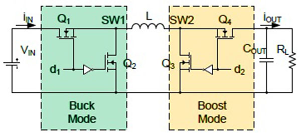 |
Fig. (1) FSBB converter. |
Fig. (1 ) shows the schematic diagram of single inductor four switch buck-boost converter, Q1 and Q3 are main power tubes, Q2 and Q4 are synchronous rectifiers. Comparing with traditional control mode that Q1 and Q3 must turn on and off at the same time, the control mode that Q1 and Q3 turn on and off respectively can effectively reduce the conduction and switching loss of the converter, and improve the efficiency [9P.C. Man, and P.K.T. Mok, "Design and implementation of fully integrated digitally controlled current-mode buck converter", Circuits & Systems I Regular Papers IEEE Transactions on, vol. 58-I, no. 8, pp. 1980-1991, 2011.-11M.K. Kazimierczuk, and L.A. Starman, "Dynamic performance of PWM DC-DC boost converter with input voltage feedforward control", IEEE Trans. Circ. Syst. I Fundam. Theory Appl., vol. 46, no. 12, pp. 1473-1481, 2000.
[http://dx.doi.org/10.1109/81.809549] ].
When the input voltage is higher than the output voltage, the converter operates in buck mode [12A. Ehrhart, "Adaptive pulse skipping and adaptive compensation capacitance techniques in current-mode buck-boost DC-DC converters for fast transient response", In: Power Electronics and Drive Systems (PEDS), 2013 IEEE 10th International Conference on, IEEE, 2013, pp. 373-378.
[http://dx.doi.org/10.1109/PEDS.2013.6527047] -14J.H. Park, H. Kim, and H.J. Kim, "A current-mode non-inverting CMOS buck-boost DC-DC converter", In: Telecommunications Energy Conference, 2009. Intelec 2009., International, IEEE, 2009.
[http://dx.doi.org/10.1109/INTLEC.2009.5351900] ]; When the input voltage is lower than the output voltage, the converter operates in boost mode [15C. Yao, "A two-mode control scheme with input voltage feed-forward for the two-switch buck-boost DC–DC converter", IEEE Trans. Power Electron., vol. 29, no. 4, pp. 2037-2048, 2014.
[http://dx.doi.org/10.1109/TPEL.2013.2270014] -17N. Kondrath, and M.K. Kazimierczuk, "Control-to-output and duty ratio-to-inductor current transfer functions of peak current-mode controlled dc-dc PWM buck converter in CCM", In: IEEE International Symposium on Circuits and Systems, IEEE, 2010.
[http://dx.doi.org/10.1109/ISCAS.2010.5537022] ]; Buck-boost operating mode is joined between two operating modes to achieve smooth transitions [18M.K. Kazimierczuk, A.J. Edstrom, and A. Reatti, "Buck PWM DC-DC converter with reference-voltage-modulation feedforward control", In: Circuits and Systems, 2001. ISCAS 2001. The 2001 IEEE International Symposium on, vol. 2. IEEE, 2001, pp. 537-540.
[http://dx.doi.org/10.1109/ISCAS.2001.921366] , 19R.W. Erickson, Fundamentals of Power Electronics, CRC Press: USA, 2000, pp. 187-263.].
2. TRANSITION PRINCIPLE OF OPERATING MODES
Fig. (2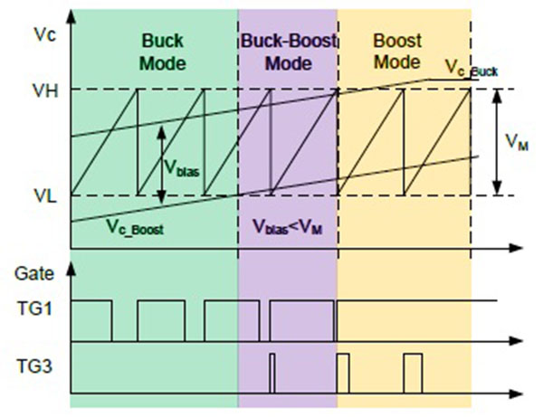 ) shows the operation schematic diagram of double modulation-single carrier three mode transitions. Vc_Buck and Vc_Boost are control signals for buck and boost respectively, Vbias is the bias between the two control signals and VM is the amplitude of carrier wave. Where Vc_Buck = Vc_Boost + Vbias, Vbias < VM
 |
Fig. (2) Switching schematic diagram of operating mode. |
When VL < Vc_Buck < VH, Vc_Boost < VL, the converter is on buck mode, duty ratio d1, which is needed in this mode, is generated through contrasting Vc_Buck and carrier signal, thus Q3 open and Q4 close. When VL < Vc_Buck < VH, VL < Vc_Boost < VH, the converter is on buck-boost mode, duty ratio d1 and d2, which are needed in this mode, is generated through contrasting Vc_Boost, Vc_Buck and carrier wave; When VH < Vc_Buck, VL < Vc_Boost < VH, the converter is on boost mode, while Q1 close and Q2 open, duty ratio d2 is generated through contrasting Vc_Boost and carrier wave [12A. Ehrhart, "Adaptive pulse skipping and adaptive compensation capacitance techniques in current-mode buck-boost DC-DC converters for fast transient response", In: Power Electronics and Drive Systems (PEDS), 2013 IEEE 10th International Conference on, IEEE, 2013, pp. 373-378.
[http://dx.doi.org/10.1109/PEDS.2013.6527047] , 13G.T. Bae, and F.S. Kang, "Bidirectional DC-to-DC converter employing a selective switch and two inductors for optimal operation in buck and boost mode", In: International Conference on Electrical Machines and Systems, IEEE, 2013.
[http://dx.doi.org/10.1109/ICEMS.2013.6713322] ].
Fig. (3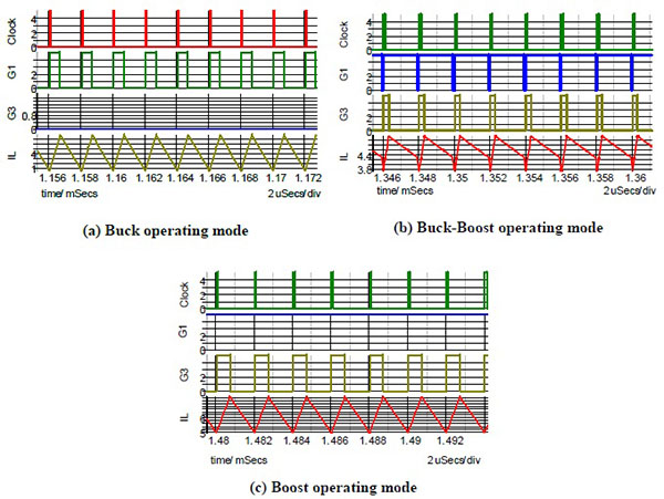 ) shows the simulation wave of those three operating modes, G1 and G3 are driver signals for Q1 and Q3 respectively, IL is inductance current waveform.
The simulation wave of converter is shown as Fig. (3a) when input voltage Vin=20V,output voltage Vout=12V, load Iout=4A, and converter is on buck mode.
The simulation waves of converter are shown as Fig. (3b) when Vin=11V, Vout=12V, Iout=4A and converter is on buck-boost mode. The simulation waves of converter are shown as Fig. (3c) when Vin=8V, Vout=12V, Iout=4A and converter is on boost mode.
Though the simulation waves, we can see that comparing with traditional control mode, this working mode has lower switching loss when converter works on Buck or Boost mode, and lower conduction loss for the lower current effective value when the converter works on Buck-Boost mode.
 |
Fig. (3) Three working modes. |
3. CONTROLLING STRATEGY AND MODELING FOR SINGLE-INDUCTOR FSBB CONVERTER
Fig. (4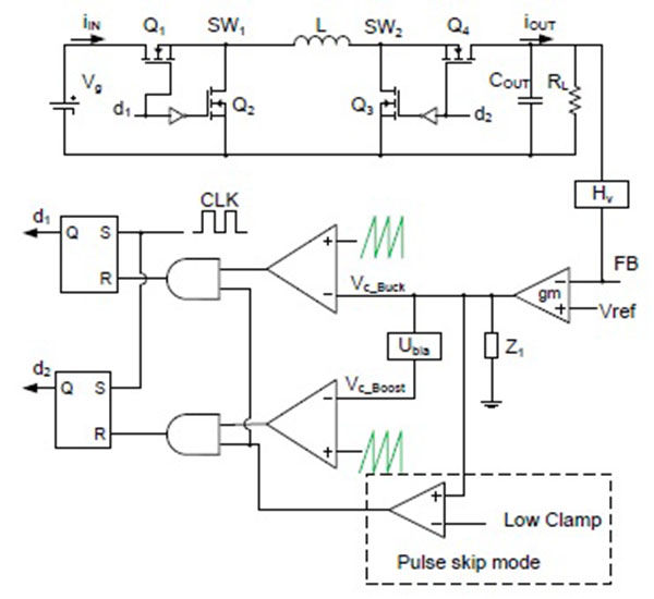 ) shows the schematic diagram of voltage mode control FSBB converter. It can be seen from the figure that the output of the error amplifier generates two modulating signals, Vc_buck and Vc_boost through the bias voltage, and the needed driver signal is generated by the contrast between these two modulating signals and the same carrier signal. In order to restrain input voltage influence on output voltage [14J.H. Park, H. Kim, and H.J. Kim, "A current-mode non-inverting CMOS buck-boost DC-DC converter", In: Telecommunications Energy Conference, 2009. Intelec 2009., International, IEEE, 2009.
[http://dx.doi.org/10.1109/INTLEC.2009.5351900] -16U. Nasir, Z. Iqbal, M.T. Rasheed, and M.K. Bodla, "Voltage mode controlled buck converter under input voltage variations", In: IEEE International Conference on Environment and Electrical Engineering, IEEE, 2015.
[http://dx.doi.org/10.1109/EEEIC.2015.7165298] ], we introduce feed forward control and make input voltage constitute carrier signal through a integral circuit. When input voltage change, control signal can also rapidly change to restrain the influence of input voltage disturbance.
 |
Fig. (4) FSBB converter based on voltage mode control. |
Equation (1) shows the formula of carrier signal:
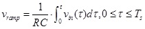 |
(1) |
When input voltage held constant, carrier signal Vramp is a set of periodic saw tooth signal, duty ratio control signal d1 and d2 are generated by modulating signal, Vc_Buck and Vc_Boost and carrier signal Vramp. Equation (2) shows the formula of PWM modulator:
 |
(2) |
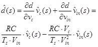
Where vc(t) denotes modulating signal, and
 is carrier slope. It can be seen from formula (2), output signal d of PWM modulator is the function of vin and vc, d = f(vc , vin), so the gain expression of PWM modulator in complex frequency domain is:
 |
(3) |
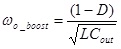
In the steady-state,
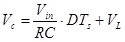 |
(4) |
VL is the low clamping voltage of Vc
Substituting (4) into (3):
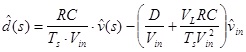 |
(5) |
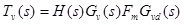
Fig. (5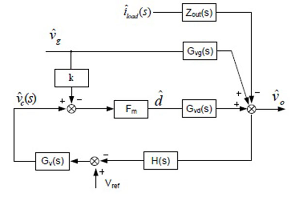 ) presents the control block diagram of converter voltage closed-loop [8M. Gaboriault, and A. Notman, "A high efficiency, noninverting, buck-boost DC-DC converter", In: Applied Power Electronics Conference and Exposition, 2004. Apec '04., Nineteenth IEEE, 2004.
[http://dx.doi.org/10.1109/APEC.2004.1296049] ]. Gvd(s), Gvg(s) and Zout(s) are the transfer functions from duty ratio
 , input voltage
 to output voltage
 and output impedance respectively, H(s) is the sampling function of output voltage, Gv(s) is the compensation function of voltage loop, Fm is the gain of PMW modulator and k is the input voltage feed forward gain.
 |
Fig. (5) FSBB converter control configuration. |
The value of the gain of PMW modulator, Fm and feedforward input voltage, k can be derived by equation (5).
 |
(6) |
 |
(7) |
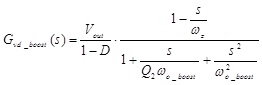
When the converter works on buck mode, transfer function from duty ratio to output voltage is:
 |
(8) |
The transfer function from input voltage to output voltage is:
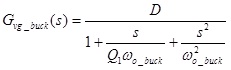 |
(9) |
Where
 ,
,
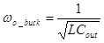
When the converter works on boost mode, transfer function from duty ratio to output voltage is:
 |
(10) |
The transfer function from input voltage to output voltage is:
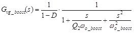 |
(11) |
Where
 ,
,
 ,
,
 .
.
The buck-boost working mode is the transition stage between buck and boost mode, and it has similarity on control loop with boost mode, so we take buck-boost working mode into boost mode to analyze.
Whether converter works on Buck mode or Boost mode, the system is a second-order system; in order to guarantee the stability of the converter, we use III type compensator to compensate converter. Fig. (6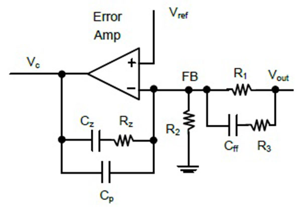 ) gives the type-III compensator.
Complex frequency domain expression of the type-III compensator is:
 |
(12) |
 |
Fig. (6) Type-III compensator. |
Pole at the base point of the compensator raises DC gain of the system, and reduces the steady state error of converter output voltage. Setting the two zero points at prior to the LC resonant frequency reduces influence of the system LC pole pair, and improves the phase margin. Setting the two poles at the rear of the half switching frequency, the two high-frequency poles rapidly downgrade high frequency gain and restrain high frequency noise.
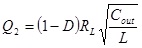
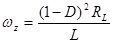
To stabilize the buck and boost mode, we need to minish the Q value of buck and boost mode in addition to the compensation. Equations (8) and (10) above have made it clear that one needs to decrease the output capacitance or increase inductance to minish Q value. In the boost mode, however, an increased inductance would lead to shift of the right half plane zero point toward low frequency, thus causing decrease of phase margin and instability of boost mode. Therefore, the value of inductance should be modest.
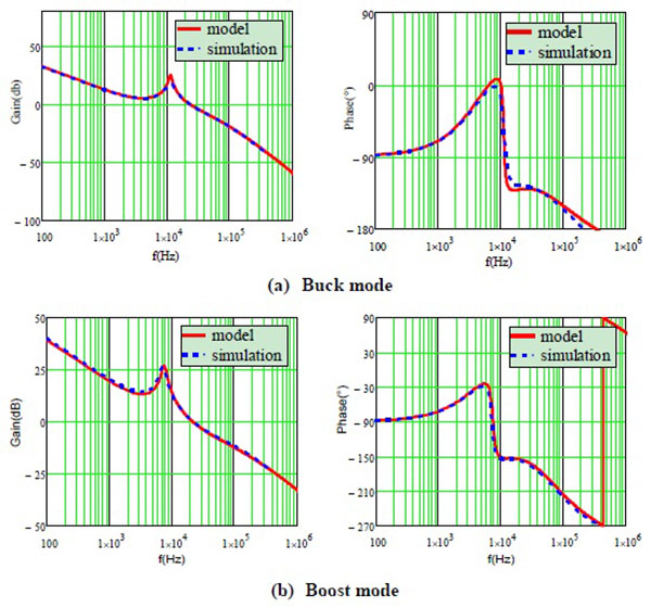 |
Fig. (7) Modeling and simulation Bode diagram under different modes. |
As shown in Fig. (7a ), the Bode diagram of loop modeling and simulation in buck mode, the small-signal model of buck mode is consistent with the simulation, indicating that the small-signal model is precise. Here the cross-over frequency fc = 22kHz, and the phase margin Pm = 53°.
As shown in Fig. (7b), the Bode diagram of loop modeling and simulation in boost mode, the right half plane zero point restrained the phase margin raising effect brought by the feedforward capacitance compensation, leading to decrease of phase margin in boost mode. Here the cross-over frequency fc = 22kHz, and the phase margin Pm = 28°.
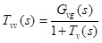
Fig. (7) indicates that cross-over frequency of the system is low in both buck mode and boost mode, thus the input voltage dynamic response is weak, and we need to introduce the input voltage to feedback loop to increase the dynamic response performance. Fig. (5) presents the block diagram of control of buck-boost converter, indicating that the open-loop gain of the voltage loop is:
 |
(13) |
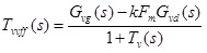
When there is no input voltage feedforward, the closed loop transfer function from input voltage to output voltage is:
 |
(14) |
When there is input voltage feedforward, the closed loop transfer function from input voltage to output voltage is:
 |
(15) |
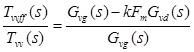
Equations (15) and (14) lead to:
 |
(16) |
When the buck-boost converter is operating in buck mode:
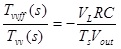 |
(17) |
When the buck-boost converter is operating in boost mode:
 |
(18) |
Low clamp value of control signal Vc is generally small during the design process. Equations (17) and (18) indicate that when the input voltage is introduced in the feedback loop, closed loop gain from input to output of buck-boost converter decreases. It is showing that the input voltage feedforward control restrained the influence of input voltage disturbance on the output voltage.
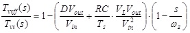
Fig. (8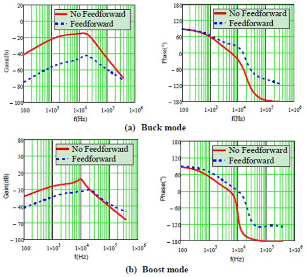 ) demonstrates the Bode diagram of closed loop transfer function from input voltage to output voltage in buck mode and boost mode. As shown in the figure, gain obviously decreases after the input voltage is added in the feedback loop, indicating that the system can effectively restrain the affect of input voltage disturbance on output voltage.
 |
Fig. (8) Bode diagram of closed loop transfer function from input voltage to output voltage under different modes. |
Fig. (9 ) illustrates the system line transient response when its input voltage is jumping between 8V-24V. The figure indicates that the system operation is shifting smoothly among the three operation modes during line transient. When input voltage jumps from 8V to 24V, converter operates in buck mode, buck-boost mode and eventually works in boost mode. When input voltage jumps from 24V to 8V, converter operates in boost mode, buck-boost mode and eventually works in buck mode. During line transient, the change of output voltage is within ±8%, which meets the system operation requirement.
 |
Fig. (9) Line transient response. |
4. EXPERIMENT VALIDATION
An experimental prototype was set in laboratory condition to verify the performance of the prototype under the control strategy proposed in the paper and the compensation parameters. Major parameters of the prototype are as follows: Vin=3V-36V, Vout=12V, L=4.4uH, Cout=44uF, Rz=50kΩ, Cz=680pF, Cff=470pF, Cp=5pF°.
Fig. (10a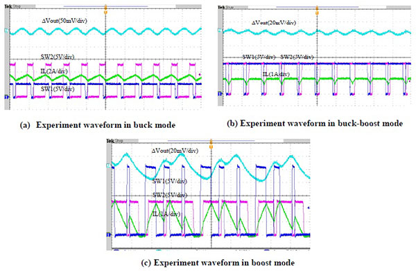 ) presents the steady state experiment waveforms under different operation modes. Fig. (10b) shows the experiment waveform under buck-boost mode, where the waveform of inductance current is a trapezoidal wave; compared to the triangular wave under the same load, the inductance current RMS value decreases, and so does the system conduction loss. Fig. (10c) presents the experiment waveform in boost mode. When the system works in light load, to reduce system loss, it works in pulse skip mode; therefore, during the critical conduction, slight vibration occurs due to the inter-affect between pulse skip loop and continuous conduction control loop.
 |
Fig. (10) Steady state experiment waveform. |
Because the buck-boost mode is actually the transition between buck mode and boost mode, it is also an unstable zone of the system. Fig. (11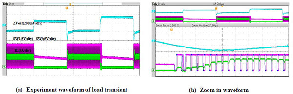 ) gives the test on load transient response in buck-boost mode. As shown in the figure, when the load jumps between 0 and 5A, the output voltage stays stable within ±5%, indicating that the system bandwidth is reasonable; in the meantime, no vibration occurs, showing that the system has enough phase margin and restrain input disturbance fine.
 |
Fig. (11) Experiment waveform of load transient. |
CONCLUSION
In the study, different operation modes of four-switch Buck-Boost (FSBB) converter were modeled, and the accuracy of the models were verified through loop simulation. Voltage mode control has weak restrain effect over input voltage disturbance. To solve the problem, we constructed carrier signal with input voltage to introduce the input voltage into feedback loop, and restrained the disturbance of input voltage. Simulations showed that, with reasonable parameter design and input voltage feedforward, the phase margin of system has been increased, and the stability was raised. At last we designed an experimental prototype with input voltage between 3V-36V and output voltage 12V for test. Test results showed that the system can shift in the three modes smoothly, that the compensation parameters were rational, that the bandwidth was high, and that the phase margin was enough.
CONFLICT OF INTEREST
The authors confirm that this article content has no conflict of interest.
ACKNOWLEDGEMENTS
This paper is supported by the Natural Science Foundation of Zhejiang province, China (Grant No. LY15E050001), and it is also supported by the Zhejiang Open Foundation of the Most Important Subjects (Grant No. ZSTUME01A07).
REFERENCES
| [1] | A. Jangwanitlert, "Analysis of a wide load variation of ZVZCS phase-shifted PWM full-bridge DC-DC converter", In: Electrical Engineering Congress (iEECON)., International, IEEE, 2014. [http://dx.doi.org/10.1109/iEECON.2014.6925836] |
| [2] | Y.P. Su, "Current-mode synthetic control technique for high-efficiency DC–DC boost converters over a wide load range", IEEE Trans. Very Large Scale Integr. (VLSI) Syst., vol. 22, no. 8, pp. 1666-1678, 2014. [http://dx.doi.org/10.1109/TVLSI.2013.2277491] |
| [3] | C.Y. Ho, "Advance semiconductor package applied on high efficiency dual-mode DC-DC buck converter", In: International Conference on Electronic Packaging Technology, IEEE, 2015. [http://dx.doi.org/10.1109/ICEPT.2015.7236571] |
| [4] | Y.J. Lee, A. Khaligh, and A. Emadi, "A compensation technique for smooth transitions in non-inverting buck-boost converter", IEEE Trans. Power Electron., vol. 24, no. 4, pp. 1002-1015, 2009. [http://dx.doi.org/10.1109/TPEL.2008.2010044] |
| [5] | B. Sahu, and G.A. Rincon-Mora, "A low voltage, dynamic, noninverting, synchronous buck-boost converter for portable applications", IEEE Trans. Power Electron., vol. 19, no. 2, pp. 443-452, 2004. [http://dx.doi.org/10.1109/TPEL.2003.823196] |
| [6] | X. Ren, X. Ruan, H. Qian, M. Li, and Q. Chen, "Dual-edge modulated four-switch Buck-Boost converter", In: Power Electronics Specialists Conference, IEEE, 2008, pp. 3635-3641. |
| [7] | H. Qiao, "Analysis of buck-boost converters for fuel cell electric vehicles", In: IEEE International Conference on Vehicular Electronics and Safety, IEEE, 2006. [http://dx.doi.org/10.1109/ICVES.2006.371564] |
| [8] | M. Gaboriault, and A. Notman, "A high efficiency, noninverting, buck-boost DC-DC converter", In: Applied Power Electronics Conference and Exposition, 2004. Apec '04., Nineteenth IEEE, 2004. [http://dx.doi.org/10.1109/APEC.2004.1296049] |
| [9] | P.C. Man, and P.K.T. Mok, "Design and implementation of fully integrated digitally controlled current-mode buck converter", Circuits & Systems I Regular Papers IEEE Transactions on, vol. 58-I, no. 8, pp. 1980-1991, 2011. |
| [10] | R. Paul, and D. Maksimovic, "Smooth transition and ripple reduction in 4-switch non-inverting buck-boost power converter for WCDMA RF power amplifier", In: IEEE International Symposium on Circuits and Systems, 2008, pp. 3266-3269. [http://dx.doi.org/10.1109/ISCAS.2008.4542155] |
| [11] | M.K. Kazimierczuk, and L.A. Starman, "Dynamic performance of PWM DC-DC boost converter with input voltage feedforward control", IEEE Trans. Circ. Syst. I Fundam. Theory Appl., vol. 46, no. 12, pp. 1473-1481, 2000. [http://dx.doi.org/10.1109/81.809549] |
| [12] | A. Ehrhart, "Adaptive pulse skipping and adaptive compensation capacitance techniques in current-mode buck-boost DC-DC converters for fast transient response", In: Power Electronics and Drive Systems (PEDS), 2013 IEEE 10th International Conference on, IEEE, 2013, pp. 373-378. [http://dx.doi.org/10.1109/PEDS.2013.6527047] |
| [13] | G.T. Bae, and F.S. Kang, "Bidirectional DC-to-DC converter employing a selective switch and two inductors for optimal operation in buck and boost mode", In: International Conference on Electrical Machines and Systems, IEEE, 2013. [http://dx.doi.org/10.1109/ICEMS.2013.6713322] |
| [14] | J.H. Park, H. Kim, and H.J. Kim, "A current-mode non-inverting CMOS buck-boost DC-DC converter", In: Telecommunications Energy Conference, 2009. Intelec 2009., International, IEEE, 2009. [http://dx.doi.org/10.1109/INTLEC.2009.5351900] |
| [15] | C. Yao, "A two-mode control scheme with input voltage feed-forward for the two-switch buck-boost DC–DC converter", IEEE Trans. Power Electron., vol. 29, no. 4, pp. 2037-2048, 2014. [http://dx.doi.org/10.1109/TPEL.2013.2270014] |
| [16] | U. Nasir, Z. Iqbal, M.T. Rasheed, and M.K. Bodla, "Voltage mode controlled buck converter under input voltage variations", In: IEEE International Conference on Environment and Electrical Engineering, IEEE, 2015. [http://dx.doi.org/10.1109/EEEIC.2015.7165298] |
| [17] | N. Kondrath, and M.K. Kazimierczuk, "Control-to-output and duty ratio-to-inductor current transfer functions of peak current-mode controlled dc-dc PWM buck converter in CCM", In: IEEE International Symposium on Circuits and Systems, IEEE, 2010. [http://dx.doi.org/10.1109/ISCAS.2010.5537022] |
| [18] | M.K. Kazimierczuk, A.J. Edstrom, and A. Reatti, "Buck PWM DC-DC converter with reference-voltage-modulation feedforward control", In: Circuits and Systems, 2001. ISCAS 2001. The 2001 IEEE International Symposium on, vol. 2. IEEE, 2001, pp. 537-540. [http://dx.doi.org/10.1109/ISCAS.2001.921366] |
| [19] | R.W. Erickson, Fundamentals of Power Electronics, CRC Press: USA, 2000, pp. 187-263. |