- Home
- About Journals
-
Information for Authors/ReviewersEditorial Policies
Publication Fee
Publication Cycle - Process Flowchart
Online Manuscript Submission and Tracking System
Publishing Ethics and Rectitude
Authorship
Author Benefits
Reviewer Guidelines
Guest Editor Guidelines
Peer Review Workflow
Quick Track Option
Copyediting Services
Bentham Open Membership
Bentham Open Advisory Board
Archiving Policies
Fabricating and Stating False Information
Post Publication Discussions and Corrections
Editorial Management
Advertise With Us
Funding Agencies
Rate List
Kudos
General FAQs
Special Fee Waivers and Discounts
- Contact
- Help
- About Us
- Search


The Open Ceramic Science Journal
(Discontinued)
ISSN: 1876-3952 ― Volume 2, 2013
Structural and Electrical Properties of Reaction Bonded Silicon Nitride Ceramics
Hosneara1, Abul Hasnat*, 2, Abu Hasan Bhuyan3
Abstract
The effects of structural properties on the d.c. and a.c. electrical properties of different weight gain reaction bonded silicon nitride (RBSN) have been studied in this work. The degree of nitridation is assessed by the ‘weight gain’ of the ceramic, the percentage by which the weight is increased in the nitriding reaction. From X-ray diffraction (XRD) patterns, it is observed that a higher degree of nitriadation sample has strong α-silicon nitride peaks. Intensity of α-silicon nitride peaks decreases with decreasing weight gain. The higher degrees of nitridation, the samples have less significant Si peak. XRD patterns were recorded to calculate the lattice parameters of RBSN. The lattice parameters for three weight gain RBSN samples are found to be a =b = 7.7727 Å, c= 5.6565 Å (26% weight gain), a=b= 7.6272 Å, c= 5.6374 Å (42% weight gain) and a=b=7.6158 Å, c= 5.7732 Å (58.27% weight gain) and are in good agreement with the reported values from XRD patterns. Porosity (%) and surface morphology was observed by SEM.
Article Information
Identifiers and Pagination:
Year: 2012Volume: 2
First Page: 1
Last Page: 7
Publisher Id: TOCERSJ-2-1
DOI: 10.2174/1876395201202010001
Article History:
Received Date: 20/5/2011Revision Received Date: 02/8/2011
Acceptance Date: 30/8/2011
Electronic publication date: 18/01/2012
Collection year: 2012
open-access license: This is an open access article distributed under the terms of the Creative Commons Attribution License (http://creativecommons.org/licenses/by/2.5/), which permits unrestrictive use, distribution, and reproduction in any medium, provided the original work is properly cited.
* Address correspondence to this author at the Department of Physics, Jagannath University, Dhaka, Bangladesh; Tel: 01818335620; E-mail mahasnat.phy@gmail.com
| Open Peer Review Details | |||
|---|---|---|---|
| Manuscript submitted on 20-5-2011 |
Original Manuscript | Structural and Electrical Properties of Reaction Bonded Silicon Nitride Ceramics | |
1. INTRODUCTION
Silicon nitride (Si3N4) is one of the most promising ceramic materials that was developed in the 1960’s and 70 s in a search for fully dense, high strength and high toughness materials. As a high temperature engineering ceramic attract more attention because of its promising thermo mechanical properties such as high temperature mechanical strength, durability, thermal shock resistance and chemical corrosion resistance etc. Also Si3N4 is a potentially high thermal conductivity material with an intrinsic value of up to 200Wm-1K-1. Silicon nitride is being considered for a wide variety of structural applications, hot flow-path components for gas turbine engine, turbocharger rotors and diesel engine components. A major application of silicon nitride ceramic aimed for in the construction of a gas turbine engine. If the target is realized, fuel saving of up to 40% for a given power output is possible. In addition, the engine would be lighter and constructed from cheap and readily available materials [1]. Although the ultimate goal of a ceramic has never been achieved, silicon nitride has been used in a number of industrial applications, such as engine components, bearings and cutting tools.Si3N4 can be hot pressed (HPSN) to full density such materials exhibit good low temperature mechanical properties. However, because a hot-pressing aid is used, the high temperature properties may be severally degraded (the severity depends on the type and amount of additive). Furthermore, Si3N4 can only be hot pressed in simple configuration. While diamond – grinding might be used to form complex components, its cost would be prohibitive for most applications. Si3N4 also can be cold formed and sintered (SSN) near to full density however, sintering aids must be used in large quantities which can lead to the deterioration of high temperature properties as in the case of hot- pressed Si3N4[2, 3]. The most commonly used additives are magnesium oxide (MgO) and yttrium oxide (Y2O3), which can be used separately, in combination or with aluminum oxide (Al2O3). Interest in RBSN as a high-temperature engineering ceramics was first shown about twenty years ago by Norman Parr of the admiralty Materials laboratory and Popper [4, 5] of the British Ceramic Research Association, in United Kingdom. RBSN produced by reaction bonding of silicon powder compacts is cheaper compared to sintered Si3N4, because the price of Si powder is much lower than that of Si3N4 powder. Reaction bonding processes generally require lower fabrication temperatures than hot pressing and pressure less sintering which is a potential advantage for processing ceramic-matrix composites where high temperatures can damage the reinforcement phase [6, 7].
2. MATERIALS AND METHODS
Scanning Electron Microscope (SEM) was used to observe the surface morphology. For D.C. electrical measurement of RBSN, electroding, Keithly 614 electrometer, D.C. power supply, specimen chamber, and heating coil are used. A Brief description of these instruments is given below. The Agilent 4192 A Impedance Analyzer (5Hz – 13 MHz) was used in the A.C. measurement. This instrument can measure various parameters; resistance (R), Conductivity (G) etc. The following ac electrical parameters will be measured at different frequencies and temperatures: i) ac capacitance (Cp) and ii) ac conductance (Gp). Then ac electrical conductivity (σac), dielectric constant (ϵ') and loss tangent (tan() will be calculated. These measurements were taken against the frequency value from 5Hz to 13 MHz. During the observations for different frequencies of a sample a particular temperature was maintained. The calculations were performed using the observed values of conductance (Gp) and capacitance (Cp) at different frequencies and temperatures by the following relations for conductivity σac = (d/A Gp), where Gp = conductance, d = thickness of the sample and A= area of the electrode area. For dielectric constant ϵ' = Cp×(d/Aϵo), where Cp = capacitance of the sample, ϵo= permittivity of free space. For dielectric loss tangent tanδ = Gp/(2πfCp)., where f =linear frequency. For morphology investigation, the different weight gain RBSN samples are examined with scanning electron microscope Philips XL30 (Nether land). A study on microstructure is done by SEM observation.
3. RESULTS & DISCUSSION
3.1. SEM Analysis
SEM micrographs of different RBSN samples are shown in Figs. (1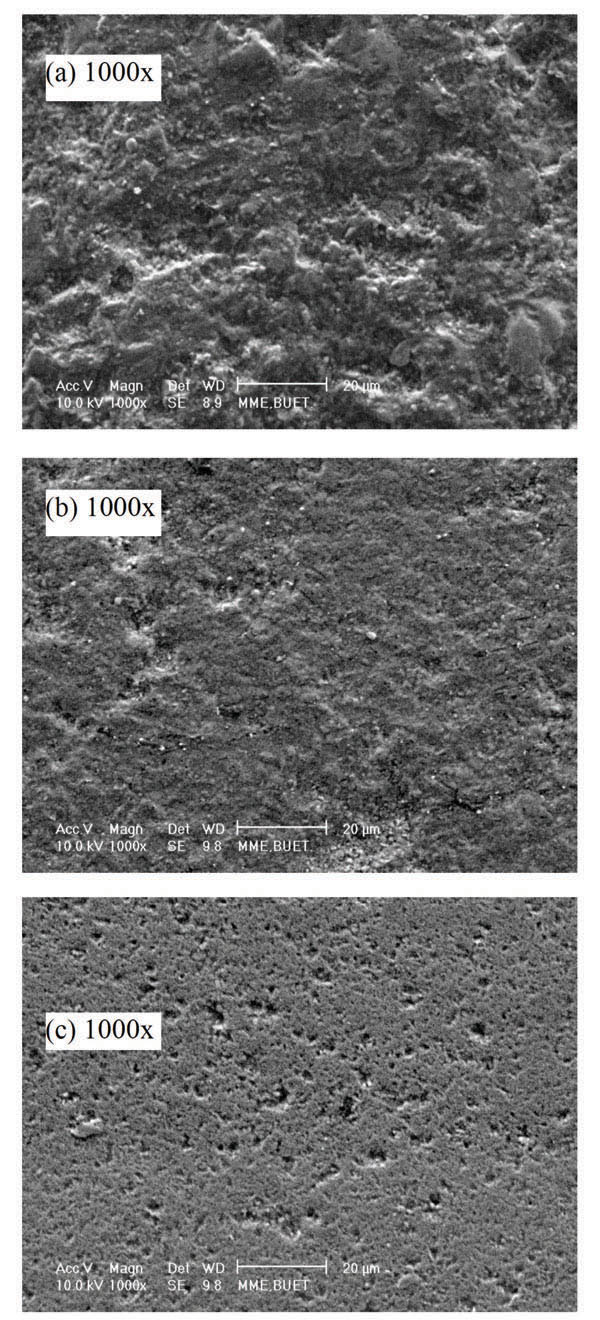 , 2
, 2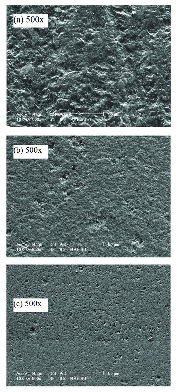 ). of 100x and 500x magnification respectively.
 |
Fig. (1) SEM micrographs of the RBSN samples (a) 26% weight gain (b) 42% weight gain and (c) 58.27% weight gain (1000 magnification). |
 |
Fig. (2) SEM micrographs of the RBSN samples (a) 26% weight gain (b) 42% weight gain and (c) 58.27% weight gain (500 magnifications). |
The samples exhibited a typical development of RBSN with porous microstructure. The micrographs of 26% weight gain sample in Figs. (1a, 2a), it is observed that the surface is rough and porous. The developments of large pores are shown in Figs. (1a, 2a), for 26% weight gain sample. From SEM micrographs of different weight gain samples, it is observed that the porosity decreases with increasing weight gain and the surface of the samples becomes smother. These facts support the observations by SEM.
3.2. XRD Analysis
X-ray diffraction (XRD) patterns of different weight gain RBSN samples are presented in Fig. (3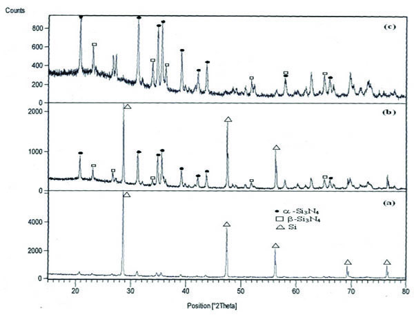 ). The XRD pattern of 26% weight gain sample has strong silicon peaks and less significant α and β- silicon nitride peaks. The XRD patterns of 42% weight gain sample has silicon and α and β- silicon nitride peaks. The XRD patterns of 58.27% weight gain sample exhibits β-silicon nitride peaks and strong α- silicon nitride peaks. It could be noticed that there is increase in peak intensity of α- and β-silicon nitride with the increase of weight gain %. It is observed that the peak intensity of α- silicon nitride phase is stronger in 58.27% weight gain sample than those in other samples. A distinct feature of the nitridation of Si is that both α and β phases are always simultaneously formed, that is, the Si3N4 product usually consist of both α and β phases. Moulson [4] proposed that major growth of β-phase occurs in the liquid phase and to a minor extent, as a result of the reaction of solid silicon and nitrogen and the growth of α-phase occurs by vapor phase reaction. α- and β- Si3N4 are polymorphs of Si3N4 with α-Si3N4 having slightly higher free energy at the formation temperature. RBSN sample crystallizes in the hexagonal system. From XRD results, lattice parameters were calculated using the formula for hexagonal system. The calculated lattice parameters a, b and c are shown in Table 1. Experimental values of lattice parameters are very close to the reported standard values [7] as mentioned below. The volumes of the unit cells of different samples are given in Table 1.
 |
Fig. (3) XRD Patterns of (a) 26% weight gain, (b) 42% weight gain, (c) 58.27% weight gain RBSN samples. |
Porosity was calculated from XRD patterns by using the formula,
Porosity of different weight gain samples are shown in Table 2.
It is observed that porosity decreases with increasing weight gain.
3.3. Current Density
The variation of voltage of current density for 26% weight gain sample is shown in Fig. (4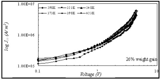 ). From this figure, it is observed that current density increases with increasing voltage. The applied voltage is 0 to 5 V. The current density is weakly dependent on temperature.
 |
Fig. (4) Current density as a function of applied voltage. |
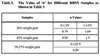
Current density as a function of applied voltage for 42% weight gain sample is shown in Fig. (5a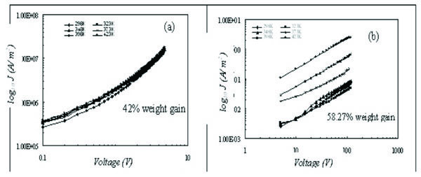 ). It is shown that current density increases with increasing voltage and also slightly increases with temperature. The also the applied voltage is 0 to 5 V. The variation of current density as a function of voltage for 58.27% weight gain sample is shown in Fig. (5b). From this graph it is found that current density increases with increasing voltage and temperature. Current density at higher temperature (423K) is 101 orders higher than that of lower temperature (298K). Current density at different voltages follows the J ( Vn law. The value of ‘n’ for different RBSN samples are shown in Table 3.
 |
Fig. (5) (a, b) Current density as a function of applied voltage. |
The value of n is close to unity. This means that the contact is ohmic. ‘n’ decreases with increasing weight gain.
3.4. Current Density – Temperature Characteristics
The applied voltage was kept at a constant value of 100V for 58.27% weight gain sample and 3V for 42% and 26% weight gain samples. Current density as a function of temperature of 26% weight gain sample is shown in Fig. (6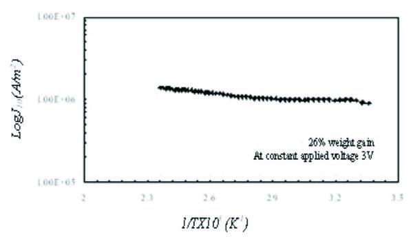 ). From this Fig., it is observed that current density increases with increasing temperature. Value of activation energies (E) were calculated from the relation J = Jo exp (- E/kT). The activation energy of 26% weight gain sample is 0.078 eV.
 |
Fig. (6) Temperature dependence current density curves. |
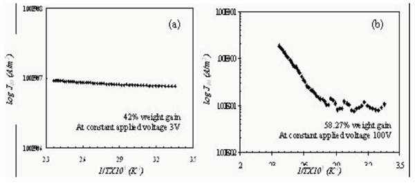 |
Fig. (7) (a, b) Temperature dependence current density curves. |
Current density vs temperature curve for 42% weight gain sample is shown in Fig. (7a ). It is found that current density increases with temperature. The activation energy of this sample is 0.03 eV. and also weakly dependent on temperature. Log J vs (1/Tx 103) curve for 58.27% weight gain is shown in Fig. (7b). It is observed that current density increases with increasing temperature. At lower temperature, the current density weakly increases with increasing temperature. The activation energy in the higher temperature region is 0.83 eV and in the lower temperature region is 0.052 eV. The activation energy is related to the formation of carriers. At lower temperature, the conduction may be due to conduction through defects states and at higher temperature the conduction may be due to electronic conduction.
3.5. A.C. Conductivity –Frequency Characteristics
A.C. conductivity (σac) as a variation of frequency for 26% weight gain sample is shown in Fig. (8a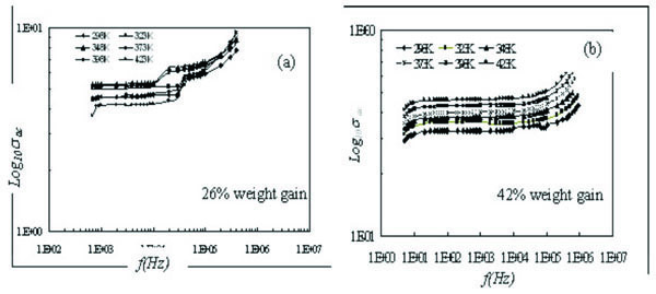 ). From this figure it is observed that σac increases with increasing frequency and is weakly dependent on temperature. The values obtained over the frequency range 5Hz-13MHz. A.C. conductivity (σac) vs frequency curve for 42% weight gain sample is shown in Fig. (8b). It is found that a.c conductivity is almost independent of frequency. A.C. Conductivity slightly increases with increasing temperature.
 |
Fig. (8) (a, b) Conductivity as a function of frequency. |
In the entire sample the σac may be affected by high frequencies. From these experimental graphs it is also found that a.c. conductivity increases with decreasing weight gain. There is a large amount of uncreated free silicon owing to the inability of nitrogen to reach the remaining silicon as the reaction progresses. Reduction of the degree of nitridation caused progressive increase in a.c. conductivity. The low conductivity material follows σac ( ωn where 0.7<n<1. These samples are weakly dependent on ‘n’. For this reason the a.c. conductivity is independent on frequency.
4. CONCLUSION
X-ray diffraction (XRD) was recorded to calculate the lattice parameters and to see the effect of nitridation, on RBSN samples. The variation of current density with voltage and temperature was measured for d.c. measurement. The a.c. electrical properties such as a.c. conductivity, dielectric constant and dielectric loss factor as functions of frequency, were investigated. The following conclusions are made from the present research work. From SEM micrographs of different weight gain samples, it is observed that the porosity decreases with increasing weight gain, and the surface of the samples becomes smother. The current density –voltage characteristics of different weight gain RBSN samples is ohmic in nature. The current density of different weight gain RBSN samples is weakly dependent on temperature. A.C conductivity σac is weakly dependent on frequency for higher weight gain samples. A.C conductivity increases with decreasing weight gain, less degrees of nitridation increases a.c. conductivity and is weakly dependent on temperature. The dielectric constant for higher degrees of nitridation samples is weakly dependent on frequency and is slightly increased by a step from 298k to 348k and becomes independent of temperature. The effects of both frequency and temperature variation are noticeably smaller on dielectric constant. This implies that the carriers make a relatively small contribution to ((. Dielectric loss factor in the higher frequency range is independent of frequency Dielectric constant and the loss factor increases progressively with the reduction of the degrees of nitridation. Less weight gain indicates that there is a large amount of uncreated free silicon.