- Home
- About Journals
-
Information for Authors/ReviewersEditorial Policies
Publication Fee
Publication Cycle - Process Flowchart
Online Manuscript Submission and Tracking System
Publishing Ethics and Rectitude
Authorship
Author Benefits
Reviewer Guidelines
Guest Editor Guidelines
Peer Review Workflow
Quick Track Option
Copyediting Services
Bentham Open Membership
Bentham Open Advisory Board
Archiving Policies
Fabricating and Stating False Information
Post Publication Discussions and Corrections
Editorial Management
Advertise With Us
Funding Agencies
Rate List
Kudos
General FAQs
Special Fee Waivers and Discounts
- Contact
- Help
- About Us
- Search


The Open Materials Science Journal
(Discontinued)
ISSN: 1874-088X ― Volume 13, 2019
Research on Carrier Correlation in Ballistic Transport Nano-MOSFETs
Xiaofei Jia1, *, Liang He2
Abstract
Objective and Method:
In this paper,the experiment proved that shot noise is suppressed by Fermi and Coulomb interaction correlation. Meanwhile, the establishment of shot noise suppression factor (Fano) in ballistic transport nano-MOSFETs the Coulomb interaction correlation and the combination of the two effects are derived from separately considering the Fermi interaction correlation. And on this basis the variation of Fano with voltage, doping concentration and temperature are investigated.
Result:
The result we obtained which considered the combination of the two effects is in good agreement with experimental studies in the research papers, thus getting a theoretical explanation for the variation of the suppression factor with the bias voltage. Meanwhile, the suppression factor model is suitable for nano-MOSFET.
Article Information

Identifiers and Pagination:
Year: 2017Volume: 11
First Page: 38
Last Page: 46
Publisher Id: TOMSJ-11-38
DOI: 10.2174/1874088X01711010038
Article History:
Received Date: 06/03/2017Revision Received Date: 21/06/2017
Acceptance Date: 30/07/2017
Electronic publication date: 22/09/2017
Collection year: 2017
open-access license: This is an open access article distributed under the terms of the Creative Commons Attribution 4.0 International Public License (CC-BY 4.0), a copy of which is available at: (https://creativecommons.org/licenses/by/4.0/legalcode). This license permits unrestricted use, distribution, and reproduction in any medium, provided the original author and source are credited.
* Address correspondence to this author at the College of Electronic and Information Engineering, Ankang University, AnKang 725000, P.R. China; Tel: ????????; E-mail: jiaxiaofei-ab@163.com
| Open Peer Review Details | |||
|---|---|---|---|
| Manuscript submitted on 06-03-2017 |
Original Manuscript | Research on Carrier Correlation in Ballistic Transport Nano-MOSFETs | |
1. INTRODUCTION
With the shortening of the channel length of MOSFET, the mechanism of the carrier has been changed as it passes through the channel. The carriers are drift-diffusive transport in long channel MOSFET, which is the result of a large number of carriers scattering in the field of electric field, thus the current noise is mainly thermal noise [1Zhuang YQ, Sun Q. The noise of the semiconductor device and low noise technology. National defense industry: Beijing 1999.]. When the channel length is in the range of sub 100 nm, carrier transport mechanism shifts from drift diffusive to quasi-ballistic or even to ballistic transport (Quasi-ballistic transport means less carrier scattering times; ballistic transport is limiting case that the carrier shot noise [2Xu W, Wong H, Kakushima K, Iwai K. Quasi-analytical model of ballistic cylindrical surrounding gate nanowire MOSFET. Microelectron Eng 2015; 138: 111-7.
[http://dx.doi.org/10.1016/j.mee.2015.03.002] -9Jia XF, He L. Research on shot noise suppression in realistic nano-MOSFETs based on Monte Carlo Simulation. Sci Sin Phys Mech Astron 2013; 47(7): 866-75.
[http://dx.doi.org/10.1360/132012-889] ]. The research has demonstrated the role of the Fermi and Coulomb correlations in the nano-MOSFET, and the simulation has been carried out [6Mugnaini G, Iannaccone G. Channel noise modelling of nanoMOSFETs in a partially ballistic transport Regime. J Comput Electron 2006; 5(2): 91-5.
[http://dx.doi.org/10.1007/s10825-006-8825-2] , 7Iannaccone G. Analytical and numerical investigation of noise in nanoscale ballistic field effect transis Tors. J Comput Electron 2004; 3(3): 199-202.
[http://dx.doi.org/10.1007/s10825-004-7044-y] , 10Betti A, Fiori G, Iannaccone G. Statistical theory of shot noise in quasi-1D Field Effect Transistors in the presence of electron-electron interaction. Phys Rev B 2010; 81(3): 1718-28.
[http://dx.doi.org/10.1103/PhysRevB.81.035329] ]. The Fermi correlation effects carrier injection in the contact side, and the higher carriers degenerate, the stronger the suppression of Fermi on the shot noise;the Coulomb correlation can change carriers, and the stronger the space charge effect, the stronger the suppression of Coulomb on the shot noise .
Although it can be concluded from the experimental results and the simulation results that shot noise is suppressed in nano-MOSFET [3Navid R, Jungemann C, Lee T, Dutton RW. High-frequency noise in nanoscale metal oxide semicon ductor field effect transistors. J Appl Phys 2007; 101(12): 124501-8.
[http://dx.doi.org/10.1063/1.2740345] , 4Andersson S, Svensson C. Direct experimental verification of shot noise in short channel MOS tran Sisters. Electron Lett 2005; 41(15): 869-71.
[http://dx.doi.org/10.1049/el:20051474] , 6Mugnaini G, Iannaccone G. Channel noise modelling of nanoMOSFETs in a partially ballistic transport Regime. J Comput Electron 2006; 5(2): 91-5.
[http://dx.doi.org/10.1007/s10825-006-8825-2] , 11Sano N, Natori K, Mukai M, Matsuzawa K. Physical mechanism of current fluctuation under ul tra-small device structures. Extended Abstracts of Sixth International Workshop on Computational Electronics 1998.], and the Fano is closely related to the device structure parameters and working parameters, there are still no suppression mechanism and shot noise suppression strength in-depth theoretical study. The research showed that noise expression in nano-MOSFET, and considering the existence of Fermi and Coulomb at the same time, only the Fermi or Coulomb interaction, or neither with simple analysis [7Iannaccone G. Analytical and numerical investigation of noise in nanoscale ballistic field effect transis Tors. J Comput Electron 2004; 3(3): 199-202.
[http://dx.doi.org/10.1007/s10825-004-7044-y] , 10Betti A, Fiori G, Iannaccone G. Statistical theory of shot noise in quasi-1D Field Effect Transistors in the presence of electron-electron interaction. Phys Rev B 2010; 81(3): 1718-28.
[http://dx.doi.org/10.1103/PhysRevB.81.035329] ]; The research established the total suppression factor formula of shot noise in ballistic MOSFET, with a simple explain and discussion on the relationship between the suppression factor and the gate voltage, but the formula for Coulomb and Fermi suppression was not analyzed respectively [6Mugnaini G, Iannaccone G. Channel noise modelling of nanoMOSFETs in a partially ballistic transport Regime. J Comput Electron 2006; 5(2): 91-5.
[http://dx.doi.org/10.1007/s10825-006-8825-2] , 7Iannaccone G. Analytical and numerical investigation of noise in nanoscale ballistic field effect transis Tors. J Comput Electron 2004; 3(3): 199-202.
[http://dx.doi.org/10.1007/s10825-004-7044-y] , 10Betti A, Fiori G, Iannaccone G. Statistical theory of shot noise in quasi-1D Field Effect Transistors in the presence of electron-electron interaction. Phys Rev B 2010; 81(3): 1718-28.
[http://dx.doi.org/10.1103/PhysRevB.81.035329] , 12Naveh Y, Korotkov AN, Likharev KK. Shot-noise suppression in multimode ballistic Fermi con Doctors. Phys Rev B 1999; 60(4): 2169-72.
[http://dx.doi.org/10.1103/PhysRevB.60.R2169] -14Michetti P, Mugnaini G, Iannaccone G. Analytical model of nanowire FETs in a partially ballistic or dissipative transport regime. Electron Dev 2009; 56(7): 1402-10.]. At present, there is no comprehensive analysis of the carrier correlation.
In this paper, firstly, the experimental results showed that the shot noise is affected by the Fermi and Coulomb interaction correlation. Then, Fano models were established with theoretical analysis of the Fermi and the Coulomb correlation. The suppression of shot noise in different situations is discussed with the variation of the bias voltage, doping concentration and temperature. Finally, the suppression results are compared with the experimental results the macroscopic shot noise suppression and the existing suppression of shot noise in the ballistic transport MOSFET.
2. EXPERIMENTAL
Select the threshold voltage of 90nm n-MOSFET device was 0.7V, the width of the device(W) is 2×10⁻⁶m, the thickness of the oxide layer is 1×10⁻⁹m, the source and drain doping concentration(NSD) is 1×1026m-3,and the noise power spectrum(S) of the device was tested under low temperature. The device works in the sub-threshold region, which is the gate voltage (VGS) is 0.25V. The variation of S with source-drain voltage (VDS) was shown in Fig. (1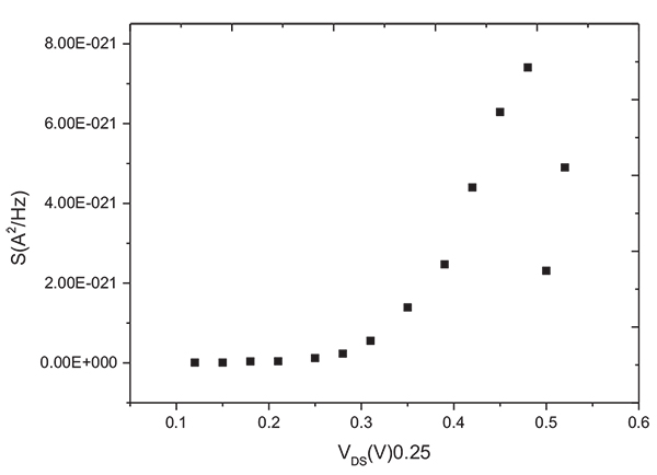 ). Then, the device works in the linear region and saturation region, which is VGS is 1.2V, as shown in Fig. (2
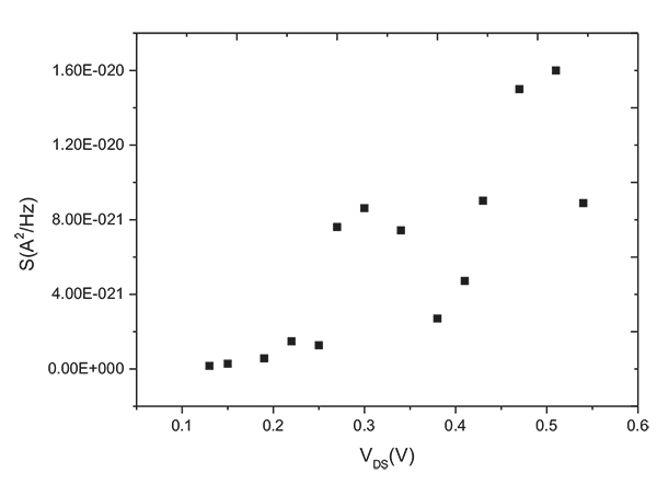 ), the S changed with VDS. As shown in figures, when the VDS is small,S is not obvious; and VDS increases, we can hear shot noise clearly, this is because the electric field increases in the channel, and lead to the barrier decreases, which means shot noise was suppressed by Fermi and Coulomb interaction correlation.
 |
Fig. (1) The variation of S with VDS. |
 |
Fig. (2) The variation of S with VDS. |
3. SHOT NOISE SUPPRESSION FACTOR MODEL
The leakage current fluctuation is the common result of the Fermi effect and potential fluctuations, which leads to the suppression of shot noise. Based on the reference [7Iannaccone G. Analytical and numerical investigation of noise in nanoscale ballistic field effect transis Tors. J Comput Electron 2004; 3(3): 199-202.
[http://dx.doi.org/10.1007/s10825-004-7044-y] ], Fano is derived in ballistic transport of nano-MOSFET. Considering the minimum sideband has been occupied, in order to simplify the formula, the following notation of  is defined:
 |
(1) |
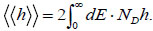
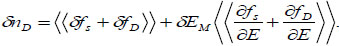
Where, h is function of kinetic energy in transport direction E. Here, ND is the electron density in the subband. The electron concentration per unit area can be expressed as:
 |
(2) |
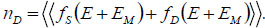
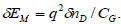
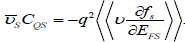
Where, fS(E) and fD(E) are the Fermi Dirac occupation factors. We assume that the fluctuations of the propagating states occupation factor affect have a direct impact on nD through electrostatic effect on EM. From (2), we can derive:
 |
(3) |
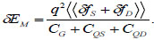
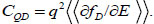
The gate capacitance per unit area CG was used to simplify the approximation of total electrostatic effects, thus the relationship between the electron density and the maximum barrier value of the side band can be expressed as:
 |
(4) |
From formula (3) and (4), it is concluded that
 |
(5) |
Where,
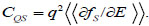 |
(6) |
 |
(7) |
When the side band barrier is maximum, the ballistic current density IB at the top of barrier is expressed as:
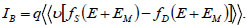 |
(8) |
As can be seen from the above formula, the fluctuations of fs, fD and EM have direct impacts on the Ballistic current.Considering the far from equilibrium case, in which fD<<1, thus fD can be discarded.
 |
(9) |
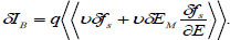
From formula (5) and (9), it is concluded that
 |
(10) |
where  is a weighted mean of the velocity:
 |
(11) |
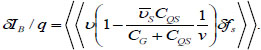
Current is the sum of the current pulses induced by all charged q, therefore 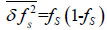 , and the occupation factor of different modes are not related. So under Fermi and Coulomb interaction correlation, the Fano is
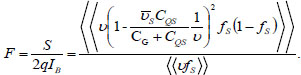 |
(12) |
Where, fs (1-fs) = fs-fs2 is Fermi interaction. When fs<<1, the small amount of high-end can be ignored, hence the formula mainly expresses Coulomb interaction correlation. Fano of the Coulomb interaction can be expressed as:
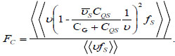 |
(13) |
where, 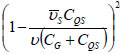 is Coulomb interaction. When
 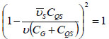 , the Fano of the Fermi interaction correlation can be expressed as:
 |
(14) |
It can be seen from the derivation of the formula that in order to get each Fano in ballistic nano- MOSFET, the top barrier energy EM should also be obtained. The gate voltage is the sum of the surface potential and the voltage drop across the oxide in ballistic transport nano-MOSFET.
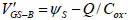 |
(15) |
Where V'GS-B = VGS-B - VFB-B, VFB-B = VT - (4ε0 εSNAΦF)1/2 / COx - 2ΦF is the flat-band voltage, COx is the oxide capacitance per unit area, and ΦF = (kT/q)ln(NA / ni), NA is channel doping concentration, ni is the intrinsic carrier density. VGS-B is the gate voltage of ballistic transport MOSFET; ΨS is the work function; Q is the charge at the top of barrier [15Lundstrom M, Guo J. Nanoscale transistors: Device physics, modeling and simulation. Beijing 2007.]. Eq. (15) can be deformed to:
 |
(16) |
EM and V'GS-B , Q are linked in formula(16). The carrier energy at the top barrier is generated by the positive emission rate of carriers in the source region and the negative emission rate of carrier in the drain region. So the top the barrier charge is also related to the top barrier potential as
 |
(17) |
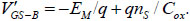
where,  is the effective density of states, EF is the Femi energy. For a given gate and drain bias, Eq. (16) and (17) define a nonlinear equation for nS (V'GS-B, VDS). Fig. (3
 ) shows the relationship between the gate voltage with top barrier potential. It can be seen from the figure that with the increase of the gate voltage, the top barrier energy decreases.
4. THE ANALYSIS OF MOEEL RESULTS
Under the Fermi interaction correlation, the Coulomb interaction correlation and the combination of the two effects, the Fano with bias voltage, doping concentration and temperature are studied separately. The channel length of the MOSFET chosen was 90nm, VDS is 0.8 V , VGS is 0.4V, temperature (T) is 300K, the source and drain doping concentration (NDS) is 1×1026m-3.
 |
Fig. (3) The variation of EM with VGS. |
4.1. Analyze the Effect of Voltage on Fano
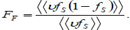
The variation of Fano with VDS was researched under the interaction of the Fermi interaction correlation, the Coulomb interaction correlation and the combination of the two effects. As shown in Fig. (4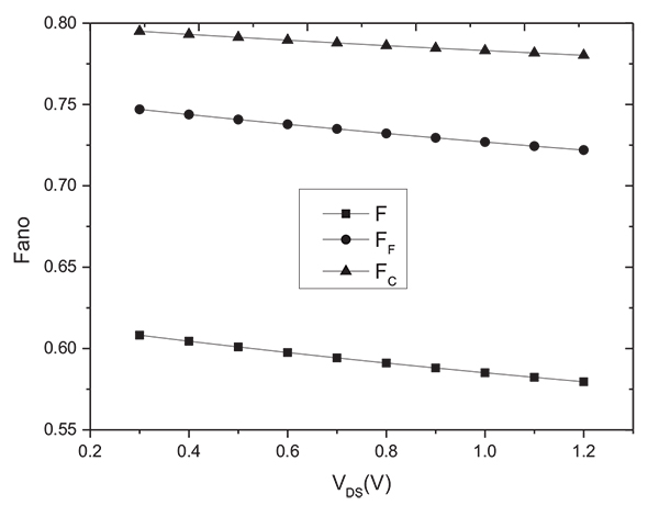 ),it can be seen that each Fano decreases with the increase of source-drain voltage, but the change is not very obvious, and the total suppression(F) is stronger than Fermi (FF)and Coulomb(FC) alone. Experiment figure showed that when VDS, the total shot noise suppression factor changed slightly the research papers [5Jeon J, Lee J, Kim J, Park CK. The first observation of shot noise characteristics in 10-nm scale MOSFETs. VLSI Technology 2009; pp. 48-50.],which is consistent with the changing trend of our theoretical results, and the theoretical explanation of the experimental results is also given.
 |
Fig. (4) The variation of Fano with VDS. |
The variation of Fano with VGS is shown in Fig. (5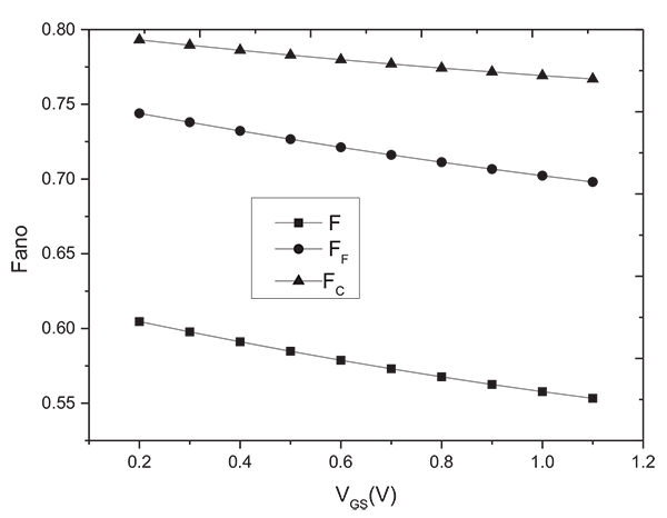 ). As the gate voltage increases, the longitudinal electric field increases, resulting in the increase of carrier surface scattering, the device transport deviates from the ballistic limit; while the electrons increase in inversion layer, and the carrier degeneracy increases, thereby enhancing the Fermi correlation to shot noise suppression [16González T, Mateos J, Pardo D, Bulashenko OM, Reggiani L. Effect of dimensionality on shot-noise suppression in nondegenerate diffusive conductors. Microelectron Reliab 2000; 40(11): 1951-4.
[http://dx.doi.org/10.1016/S0026-2714(00)00056-1] , 17Gomila G, Cantalapiedra I, González T, Reggiani L. Semiclassical theory of shot noise in ballistic n+-in-n+ semiconductor structures: Relevance of Pauli and long-range Coulomb correlations. Phys Rev B 2002; 66(7): 429-536.
[http://dx.doi.org/10.1103/PhysRevB.66.075302] ]. On the other hand, with the increase of the gate voltage,the channel barrier height reduces, the number of carriers increase, thus increasing the number of carrier inelastic scattering and the Coulomb correlation [18Naveh Y, Averin D, Likharev K. Effect of screening on shot noise in diffusive mesoscopic conductors. Phys Rev Lett 1998; 79(18): 3482-5.
[http://dx.doi.org/10.1103/PhysRevLett.79.3482] , 19Naveh Y, Averin D, Likharev K. Shot noise in diffusive conductors: A quantitative analysis of elec tron-phonon interaction effects. Phys Rev B 1998; 58(23): 15371-4.
[http://dx.doi.org/10.1103/PhysRevB.58.15371] ], leading to the suppression of shot noise. The model not only follows the shot noise suppression in mesoscopic conductors, but also the experimental trend of total suppression factor with the gate voltage [5Jeon J, Lee J, Kim J, Park CK. The first observation of shot noise characteristics in 10-nm scale MOSFETs. VLSI Technology 2009; pp. 48-50.].
 |
Fig. (5) The variation of Fano with VGS. |
4.2. Analyze the Effect of T and VDS on Fano
The increase in temperature will stop shot noise becoming the main component of noise, because the noise suppression is enhanced by temperature, which is consistent with our model. The variation of each Fano with temperature is shown in Fig. (6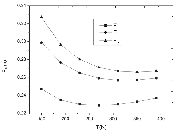 ). As shown in figure, the Fano decreases with the increase in T, and which is consistent with the conclusions in the research papers [3Navid R, Jungemann C, Lee T, Dutton RW. High-frequency noise in nanoscale metal oxide semicon ductor field effect transistors. J Appl Phys 2007; 101(12): 124501-8.
[http://dx.doi.org/10.1063/1.2740345] ]. FF and FC decrease with the increase in T in the range of 150-300K, where the channel carrier scattering is mainly acoustic wave scattering and optical wave scattering, both scattering probability of which decreases with temperature. So with temperature increase, the number of phonon scattering increases, the average number of phonons increases, leading to the enhancement of shot noise suppression [3Navid R, Jungemann C, Lee T, Dutton RW. High-frequency noise in nanoscale metal oxide semicon ductor field effect transistors. J Appl Phys 2007; 101(12): 124501-8.
[http://dx.doi.org/10.1063/1.2740345] , 20Rahman A, Lundstrom M. A compact scattering model for the nanoscale double-gate MOSFET. IEEE Trans Electron Dev 2002; 49(3): 481-9.
[http://dx.doi.org/10.1109/16.987120] -22Du L, Zhuang YQ. Nano electronics. Publishing House of Electronics Industry: Beijing 2004.]. And above 300K, Fano increases with temperature,this is because of the high temperature, the device transportation is changed from ballistic to drift-diffusion,and the device is mainly thermal noise.
 |
Fig. (6) The variation of Fano with T. |
The variation of Fano with NDS is shown in Fig. (7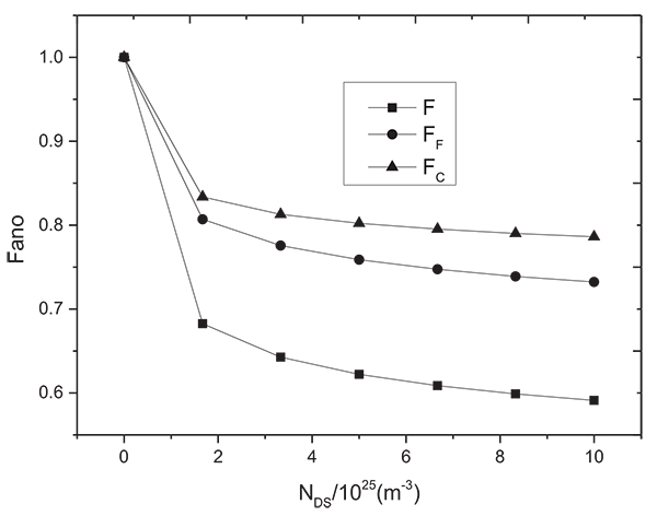 ). With NDS increases, each Fano decreases. The higher doping concentration in the source region, and the stronger shot noise are suppressed, and F is stronger than FF and Coulomb FC separately. The increase in doping concentration increases the carrier degeneracy, thus enhancing Fermi correlations. Meanwhile enhancing the space charge effect, increasing the Coulomb interaction correlation also increased [4Andersson S, Svensson C. Direct experimental verification of shot noise in short channel MOS tran Sisters. Electron Lett 2005; 41(15): 869-71.
[http://dx.doi.org/10.1049/el:20051474] , 16González T, Mateos J, Pardo D, Bulashenko OM, Reggiani L. Effect of dimensionality on shot-noise suppression in nondegenerate diffusive conductors. Microelectron Reliab 2000; 40(11): 1951-4.
[http://dx.doi.org/10.1016/S0026-2714(00)00056-1] , 17Gomila G, Cantalapiedra I, González T, Reggiani L. Semiclassical theory of shot noise in ballistic n+-in-n+ semiconductor structures: Relevance of Pauli and long-range Coulomb correlations. Phys Rev B 2002; 66(7): 429-536.
[http://dx.doi.org/10.1103/PhysRevB.66.075302] , 23Lundstrom M, Ren Z. Essential physics of carrier transport in nanoscale MOSFETs. IEEE Trans Electron Dev 2002; 49(1): 133-44.
[http://dx.doi.org/10.1109/16.974760] ].
 |
Fig. (7) The variation of Fano with NDS. |
CONCLUSION
In this paper,the experimental proved that shot noise is suppressed by Fermi and Coulomb interaction correlation in ballistic transport nano-MOSFET, and the expressions of Fano were derived with considering the Fermi interaction correlation the Coulomb interaction correlation and the combination of the two effects, respectively. The variation of each Fano with VDS, VGS, T, and NDS was studied respectively. Experimental results showed that the variation of F with VDS in ballistic nano-MOSFET was explained theoretically. The results showed that Fano decreases with increases in the voltage, the doping concentration and temperature.
ETHICS APPROVAL AND CONSENT TO PARTICIPATE
Not applicable.
HUMAN AND ANIMAL RIGHTS
No Animals/Humans were used for studies that are base of this research.
CONSENT FOR PUBLICATION
Not applicable.
CONFLICT OF INTEREST
The author declares no conflict of interest, financial or otherwise.
ACKNOWLEDGEMENTS
This work was supported by National Natural Science Foundation of China (Grant No.61106062), the Scientific Research Fund of Shaanxi Provincial Education Department(Grant No.16JK1016) and the project of Anakang University (Grant No. 2017AYQN06).
REFERENCES
| [1] | Zhuang YQ, Sun Q. The noise of the semiconductor device and low noise technology. National defense industry: Beijing 1999. |
| [2] | Xu W, Wong H, Kakushima K, Iwai K. Quasi-analytical model of ballistic cylindrical surrounding gate nanowire MOSFET. Microelectron Eng 2015; 138: 111-7. [http://dx.doi.org/10.1016/j.mee.2015.03.002] |
| [3] | Navid R, Jungemann C, Lee T, Dutton RW. High-frequency noise in nanoscale metal oxide semicon ductor field effect transistors. J Appl Phys 2007; 101(12): 124501-8. [http://dx.doi.org/10.1063/1.2740345] |
| [4] | Andersson S, Svensson C. Direct experimental verification of shot noise in short channel MOS tran Sisters. Electron Lett 2005; 41(15): 869-71. [http://dx.doi.org/10.1049/el:20051474] |
| [5] | Jeon J, Lee J, Kim J, Park CK. The first observation of shot noise characteristics in 10-nm scale MOSFETs. VLSI Technology 2009; pp. 48-50. |
| [6] | Mugnaini G, Iannaccone G. Channel noise modelling of nanoMOSFETs in a partially ballistic transport Regime. J Comput Electron 2006; 5(2): 91-5. [http://dx.doi.org/10.1007/s10825-006-8825-2] |
| [7] | Iannaccone G. Analytical and numerical investigation of noise in nanoscale ballistic field effect transis Tors. J Comput Electron 2004; 3(3): 199-202. [http://dx.doi.org/10.1007/s10825-004-7044-y] |
| [8] | Gomila G, Reggiani L. The role of boundary conditions in shot noise in elastic diffusive conductors. Semicond Sci Technol 2000; 45(15): 829-35. [http://dx.doi.org/10.1088/0268-1242/15/8/308] |
| [9] | Jia XF, He L. Research on shot noise suppression in realistic nano-MOSFETs based on Monte Carlo Simulation. Sci Sin Phys Mech Astron 2013; 47(7): 866-75. [http://dx.doi.org/10.1360/132012-889] |
| [10] | Betti A, Fiori G, Iannaccone G. Statistical theory of shot noise in quasi-1D Field Effect Transistors in the presence of electron-electron interaction. Phys Rev B 2010; 81(3): 1718-28. [http://dx.doi.org/10.1103/PhysRevB.81.035329] |
| [11] | Sano N, Natori K, Mukai M, Matsuzawa K. Physical mechanism of current fluctuation under ul tra-small device structures. Extended Abstracts of Sixth International Workshop on Computational Electronics 1998. |
| [12] | Naveh Y, Korotkov AN, Likharev KK. Shot-noise suppression in multimode ballistic Fermi con Doctors. Phys Rev B 1999; 60(4): 2169-72. [http://dx.doi.org/10.1103/PhysRevB.60.R2169] |
| [13] | Bulashenko O, Rubí J. Shot-noise suppression by Fermi and Coulomb correlations in ballistic con Doctors. Phys Rev B 2001; 64(4): 314-9. [http://dx.doi.org/10.1103/PhysRevB.64.045307] |
| [14] | Michetti P, Mugnaini G, Iannaccone G. Analytical model of nanowire FETs in a partially ballistic or dissipative transport regime. Electron Dev 2009; 56(7): 1402-10. |
| [15] | Lundstrom M, Guo J. Nanoscale transistors: Device physics, modeling and simulation. Beijing 2007. |
| [16] | González T, Mateos J, Pardo D, Bulashenko OM, Reggiani L. Effect of dimensionality on shot-noise suppression in nondegenerate diffusive conductors. Microelectron Reliab 2000; 40(11): 1951-4. [http://dx.doi.org/10.1016/S0026-2714(00)00056-1] |
| [17] | Gomila G, Cantalapiedra I, González T, Reggiani L. Semiclassical theory of shot noise in ballistic n+-in-n+ semiconductor structures: Relevance of Pauli and long-range Coulomb correlations. Phys Rev B 2002; 66(7): 429-536. [http://dx.doi.org/10.1103/PhysRevB.66.075302] |
| [18] | Naveh Y, Averin D, Likharev K. Effect of screening on shot noise in diffusive mesoscopic conductors. Phys Rev Lett 1998; 79(18): 3482-5. [http://dx.doi.org/10.1103/PhysRevLett.79.3482] |
| [19] | Naveh Y, Averin D, Likharev K. Shot noise in diffusive conductors: A quantitative analysis of elec tron-phonon interaction effects. Phys Rev B 1998; 58(23): 15371-4. [http://dx.doi.org/10.1103/PhysRevB.58.15371] |
| [20] | Rahman A, Lundstrom M. A compact scattering model for the nanoscale double-gate MOSFET. IEEE Trans Electron Dev 2002; 49(3): 481-9. [http://dx.doi.org/10.1109/16.987120] |
| [21] | Liu EK, Zhu BS, Luo JS. Physics of Semiconductor devices. National defense industry: Beijing 2006. |
| [22] | Du L, Zhuang YQ. Nano electronics. Publishing House of Electronics Industry: Beijing 2004. |
| [23] | Lundstrom M, Ren Z. Essential physics of carrier transport in nanoscale MOSFETs. IEEE Trans Electron Dev 2002; 49(1): 133-44. [http://dx.doi.org/10.1109/16.974760] |